
Aledia makes First Nanowire MicroLEDs
French developer of next-generation displays makes nanowire chips on 300mm silicon wafers using CEA-Leti pilot lines
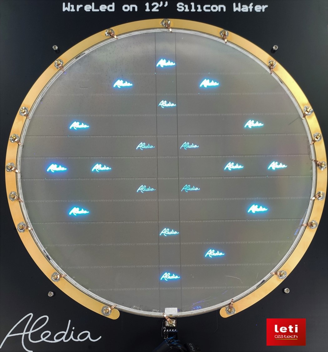
Aledia, a French startup pioneering a disruptive technology for microLED displays, today announced it has manufactured the world’s first microLED chips produced on 300mm (12”) silicon wafers. The company, which developed its breakthrough technology on 200mm (8”) silicon wafers over the past eight years, will produce the chips on both 200mm and 300mm wafers. The larger wafers provide better economic payoff and cost-effective integration with smaller-node electronics, which are only available on 300mm silicon wafers. Aledia was spun out of CEA-Leti, a French research institute pioneering micro- and nanotechnologies, in 2012, and the work on 300mm wafers has been performed by joint Aledia and CEA-Leti teams.
“We believe producing microLEDs on large-area 300mm silicon wafers is a world’s first, and opens this technology to huge potential-volume-manufacturing capabilities,” said Giorgio Anania, Aledia CEO and cofounder. “The larger size allows 60-100 smartphone displays to be made on a single 300mm wafer, versus approximately four-to-six using the present LED industry-standard, 4 inch sapphire substrate. Thanks to Aledia’s unique nanowire LED technology (3D LED), this can be done with commercially available processes and equipment, since it uses standard-thickness (780µm) silicon wafers.”
Traditional planar, 2D microLEDs are produced by depositing flat layers of GaN crystal on sapphire wafers of 100-150mm diameter (4-6 inch), with the majority of production today being on 100mm (4 inch) wafers. Aledia’s microLED technology grows GaN nanowires (GaN crystals of sub-micron diameter) on top of large-area silicon (called 3D). This 3D nanowire technology does not create any of the stresses seen on 2D chips, which build up as the wafer size is increased, and so allows the use of very large-size wafers. In addition, this silicon-based technology allows production in conventional microelectronics fabs, called silicon foundries, which can be ramped up to high volume production with extremely high yield.
“We are very pleased to have helped Aledia push forward the state of the art of 3D LED manufacturing using our 300mm silicon processing line. We believe large-area silicon wafers are the best manufacturing platform in the world today for displays, and give big advantages in manufacturability,” said Emmanuel Sabonnadière, CEO of CEA-Leti. “3D nanowire micro-LEDs have the potential to make serious penetration into large display markets. CEA-Leti is very active today in supporting the display industry’s transition to micro-LED technology.”
“We believe the use of large-area silicon wafers and microelectronics foundries are the only way to deliver the huge volumes demanded by end-user markets,” Anania said. “For example, if only the large-screen TVs of 60 inch in diagonal and larger transitioned to silicon nanowire technology to obtain better image quality and lower manufacturing costs, this would require 24 million 300mm wafers per year, volumes that can only be delivered by the silicon industry and supply chains. Smartphones, laptops and tablets would be on top of that.”
Aledia’s technology is protected by 197 patent families, making Aledia the leading French startup company in France in filed patents.
This work is sponsored by the EC: Grant Agreement number: 954553 — SPEED — H2020-EIC-SMEInst-2018-2020


