
Aledia closes in on microLED displays market
With nanowire chips demonstrated on 300 mm silicon wafers, CEA-Leti spin-out, Aledia, plans to deliver its first products next year. Rebecca Pool talks to chief executive, Giorgio Anania, to find out more.
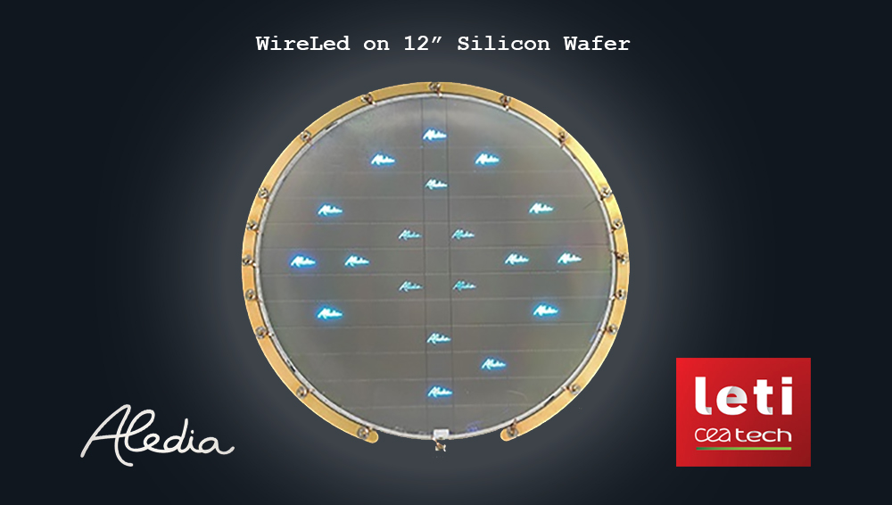
Late last year, France-based microLED display start-up, Aledia, claimed a world first by manufacturing its nanowire chips on 300 mm wafers, at its CEA-Leti pilot lines. In the last eight years, the company has been carrying out research and development on 200 mm wafers but having demonstrated the technology on the larger wafer size signals clear ambitions for volume manufacture and market entry.
As Giorgia Anania, Aledia chairman, chief executive and co-founder, tells Compound Semiconductor: “This is all about cost – we've been doing R&D on 200 mm wafer sizes as it's cheaper but, for us, the transition to larger wafer sizes is easy.”
“We'll release our first products in 2022 on 200 mm wafers, and as soon as we get into volume production the following year, we'll move to 300 mm wafers,” he adds.
Aledia's announcement comes at a time when all eyes are on MicroLEDs. Industry analysts have forecast gargantuan global microLED market growth, in the region of 90% CAGR to nearly $20 billion by 2026, as consumers demand brighter and more power-efficient display panels for smart devices and augmented/virtual reality headsets.
These mighty figures are attracting more and more businesses to the market. Key players include industry heavyweights such as Apple, Samsung, Sony, Oculus and LG Display and smaller companies and start-ups including Glo, Plessey, Play Nitride, and of course Aledia.
However, what sets the CEA-Leti spin-out apart is its technology. While most microLED developers have focused on fabricating 2D planar GaN layers on 100 mm and 150 mm sapphire substrates, Aledia has been growing GaN nanowires directly onto large-size silicon wafers. This makes technology and business sense.
For starters, growing vertical nanowires onto silicon prevents the accumulation of wafer stresses that takes place when GaN and InGaN layers are deposited on silicon or sapphire. As Anania highlights: “We don't need buffer layers and we don't have wafer bow - this allows us to transition to any wafer size.”
What's more, Aledia will eventually be able to realise the economies of scale that only silicon foundries can bring. Anania is excited.
Highlighting how the entire display market is forecast to turn around $120 billion every year, he intends for his company to target many market segments. These include TVs, laptops and tablets as well as smartphones, smartwatches and virtual/augmented reality displays. And these segments are largely driven by existing investors.
For example, Intel Capital, with its interest in laptops, tablets and mid-sized displays, has already ploughed million of dollars into Aledia. At the same time, the company also has several collaborations with unnamed smartphone and augmented reality players. As Anania points out: “This validates our technology and shows it has enormous potential for the future.”
Tackling issues
But what about the many issues that have thwarted microLED display development? From word go, display manufacturers have struggled with the mass transfer of microLEDs onto a display backplane.
However, according to Anania, Aledia is developing a parallel method to quickly and effectively transfer millions of nanowires from the wafer, directly onto the display backplane. As part of this, the company has also been working with chip-transfer equipment manufacturers to optimise transfer processes for Aledia wafers.
And while the efficiency of conventional planar microLEDs is known to swiftly drop with pixel size, Anania highlights how the efficiency of his company's nanowires remains unchanged at smaller chip sizes. Indeed, he asserts that nanowire efficiency actually exceeds that of planar micro-LEDs at sub-pixel sizes of less than 10 micron, which is critical for displays in smartphones, tablets and augmented reality devices.
“Most of the [small to mid-size] microLED display market needs 3 to 4 micron sub-pixel sizes to make money and sell at a cost that is lower than OLED displays,” he says. “So our nanowires are particularly suited to the vast number of consumer applications that we are targeting.”
Right now Aledia is developing three nanowire platforms with increasing complexity. Its initial technology comprises blue and colour-converted nanowires and is scheduled for mass production come the second half of 2022. Meanwhile the final platform, which Anania describes as 'revolutionary', will comprise red, blue and green nanowires. Volume production is scheduled to start during 2024, and once ready, this platform will replace the preceding platforms.

Aledia chief executive, Giorgio Anania.
The Aledia chief executive won't be drawn on what the company's first products will be. As he puts it: “I think we've been very clear that our high volume products will fall into the laptop segment of this market, given our collaboration with Intel.”
In the meantime, the company is very much focused on building up its manufacturing capacity. As Anania emphasises, during display manufacture Aledia only carries out the necessary nanowire growth and epitaxy, with wafer and chip processing, CMOS integration and back-end testing all taking place in silicon foundries. The company has already revealed a key partner here to be Israel-based Tower Semiconductor.
Aledia began to scale operations in late 2019, re-locating from its original Grenoble-based R&D facility at CEA-Leti to larger headquarters, and research and development facilities, still in Grenoble. And following its latest €80 million financing round, the company is building a high volume, 50,000 m2 3D microLED manufacturing facility in Grenoble - estimated to cost around €40 million - that is scheduled for completion by the second half of 2022.
“We'll be able to use our existing research and development lab for sales before this, but come the middle of 2023 we're going bigger and will need this facility to be ready for this ,” says Anania. “At this point we'll be bringing all of equipment online ready for high volumes in 2023.”
“Unlike companies, such as, say Plessey, we've spent relatively little on manufacturing and equipment in the past, relying on the national lab to do most of our processing,” he adds. “But now we're getting close to market so have been accelerating R&D, extending collaborations and buying equipment.”
Indeed, Aledia recently purchased a Veeco Propel 300 mm MOCVD system for its epitaxy. And with plans to invest a total of €200 million in equipment - including the latest expenditures - over the next five years, and grow the company to approximately 500 employees, exciting times are ahead.
“Because we're on silicon, we're currently the only company that can take advantage of the cost advantages of manufacturing on 300 mm wafer as well as sophisticated electronics integration,” highlights Anania. “This will allow us to compete aggressively and be first to market with different types of displays.”


