
Scientists map electron spins in 2D transistor
Creating an image of electron spins in MoS2 transistor may open the way for new spintronic computers
Scientists from the University of Tsukuba and a scientist from the Institute of High Pressure Physics in Poland have detected and mapped the electronic spins moving in a working transistor made of MoS2. This research may lead to much faster computers that take advantage of the natural magnetism of electrons, as opposed to just their charge.
Spintronics is a new area of condensed matter physics that attempts to use the intrinsic magnetic moment of electrons, called "spins," to perform calculations. This would be a major advance over all existing electronics that rely solely on the electron charge. However, it is difficult to detect these spins, and there are many unknowns regarding materials that can support the transport of spin-polarised electrons.
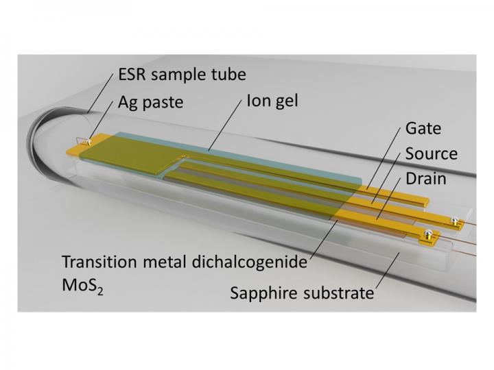
Now, an international research team led by the Division of Materials Science at the University of Tsukuba has successfully used electron spin resonance (ESR) to monitor the number and location of unpaired spins coursing through a MoS2 transistor. ESR uses the same physical principle as the MRI machines that create medical images. The spins are subject to a very strong magnetic field, which creates an energy difference between electrons with spins aligned and anti-aligned with the field. The absorbance of photons that match this energy gap can be measured to determine the presence of unpaired electron spins.
The experiment required the sample to be cooled to just four degrees above absolute zero, and the transistor to be in operation while the spins are being measured. "The ESR signals were measured simultaneously with the drain and gate currents," corresponding author Kazuhiro Marumoto says. "Theoretical calculations further identified the origins of the spins," coauthor Malgorzata Wierzbowska says. MoS2 was used because its atoms naturally form a nearly flat 2D structure. The molybdenum atoms form a plane with a layer of sulphide ions above and below.
The team found that charging the system with the additional electrons in a process called n-type doping was important for creating the spins. "In contrast with previous work on other 2D materials, the n-type doping allowed us to achieve better control of the electronic spins," Marumoto and Wierzbowska explain. The scientists believe that MoS2 will prove to be an important testbed for spintronic devices as the technology advances towards future consumer products.
'Spin-states in MoS2 thin-film transistors distinguished by operando electron spin resonance' by Naho Tsunetomo et al; Communications Materials (2021)


