
Machine-learning helps study 2D semiconductors
Australian team use machine learning to automate the characterisation of the atomically-thin material WS2
Machine-learning could identify different areas of interest on 2D semiconductors, according to a study led by Pavel Kolesnichenko at Swinburne University of Technology in Australia (and now a postdoc at Lund University in Sweden).
Their paper 'Multidimensional Analysis of Excitonic Spectra of Monolayers of Tungsten Disulphide: Towards Computer Aided Identification of Structural and Environmental Perturbations of 2D Materials' was published in Machine Learning: Science and Technology in February 2021
The simple, automated optical identification of fundamentally different physical areas on these materials (eg, areas displaying doping, strain, and electronic disorder) could significantly accelerate the science of atomically-thin materials, such as WS2.
“Without any supervision, machine-learning algorithms were able to discriminate between differently perturbed areas on a 2D semiconducting material,” explains lead author Pavel Kolesnichenko. “This can lead to fast, machine-aided characterisation of 2D materials in the future, accelerating application of these materials in next-generation low-energy smart-phones.”
Since the disocvery of graphene in 2004, dozens of other monolayers have been obtained, including metals, semiconductors, insulators, and more-exotic quantum materials such as topological-insulators, superconductors and ferromagnets.
Having this monolayer-zoo at their disposal, materials scientists have used them like ‘LEGO’-blocks: for example stacking them in many different combinations to construct next-generation transistors, batteries, memory cells and photodiodes.
All these devices, however, have been assembled manually and exist as one-off prototypes. There is still a long way towards their industrial-scale production and commercialisation.
Taking steps towards industrial-scale production
Several factors contribute to the hindrance of the progress commercialisation. First is the lack of full control over the fabrication of monolayer materials. In addition, current characterisation techniques are complicated and require the eye of an experienced researcher. Finally, due to the extreme thinness of the materials, the latter are extremely sensitive to various perturbations, many of which are introduced unintentionally. Understanding these perturbations is a non-trivial task, as they can have a combined effect and have to be disentangled.
Correlations between different experimental parameters help to identify the specific imperfections that cause variations in the optical and electronic properties across the 2D material
Pavel Kolesnichenko and Jeffrey Davis (Swinburne University of Technology) realised that the task of characterisation of 2D materials could be accomplished by machines in a rapid and automated manner.
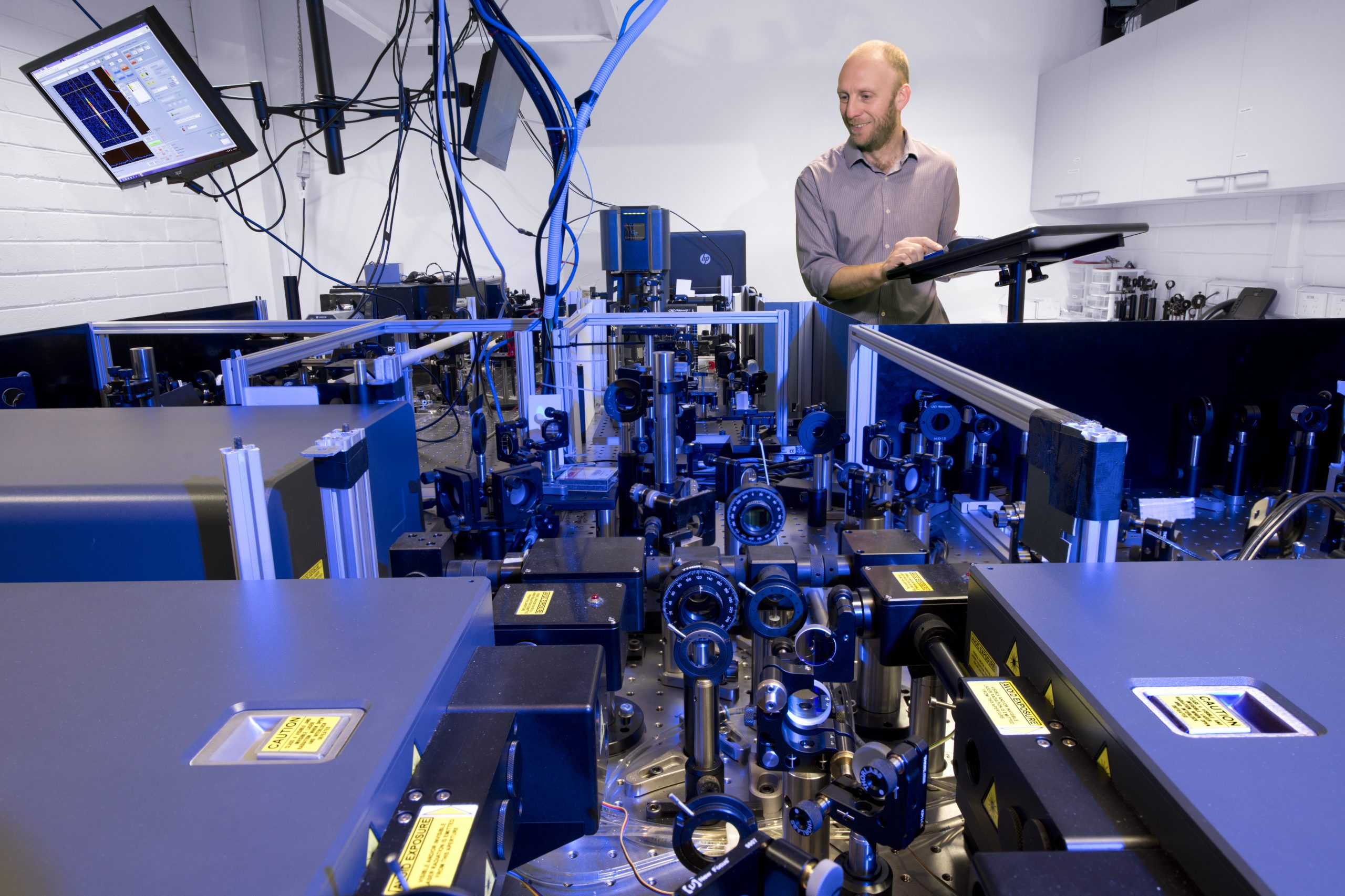
“In order to understand the impact of different perturbations and minimise or control their presence, it is important to be able to identify them and their spatial distribution rapidly and reliably,” said Davis (picture above), who is a chief investigator in ARC Centre of Excellence in Future Low-Energy Electronics Technologies (FLEET).
Working with FLEET colleague Michael Fuhrer (Monash University), they applied unsupervised machine-learning algorithms to characterize the semiconducting monolayer of tungsten disulphide. The data was acquired by simple apparatus involving a microscope and a spectrometer. The learning algorithms then were able to discriminate between the areas on a monolayer flake affected by doping, strain, disorder, and the presence of additional layers.
This is the first time such a systematic disentanglement of these perturbations has been performed.

The picture above shows correlations between different experimental parameters help to identify the specific imperfections that cause variations in the optical and electronic properties across the 2D material
The task was accomplished by embedding the acquired data into an artificially constructed multi-dimensional parameter space. Learning algorithms were then allowed to find a way to visualize the data in comprehensible two dimensions and in the most representative way, where each perturbation formed its own data-cluster.
The team built on previous scientific results in the field including their previous publication ('Disentangling the effects of doping, strain and disorder in monolayer WS2 by optical spectroscopy' published in 2D Materials in January 2020), where they disentangled perturbations using correlated photoluminescence and absorption spectra.
“So many factors can affect optoelectronic properties of 2D materials, including the type of substrate, additional doping, strain, the presence of wrinkles, defects, and environmental molecules – you name it,” said Pavel Kolesnichenko. “Thus, moving to a multi-dimensional parametric space seemed to be a natural next step.”
“We also hope the research will motivate scientists to apply similar ideas to other 2D materials and using other imaging modalities,” says Pavel.
In the era of data-driven science and technology, the authors hope that their research will motivate the creation of a large labelled dataset, where labels (such as ‘doping’, ‘strain’, etc) would be assigned by experienced researchers. This dataset would be then used to train deep neural networks to characterize 2D materials in a fraction of a second. The researchers believe that their work will help to introduce standards for characterisation of monolayer matter, approaching the moment of large-scale use of low-energy smart-phones and computers in the future.


