
Epiluvac supplies CVD reactors to Polish Research group
Lukasiewicz Research Network at the Institute of Microelectronics and Photonics to use system for 8-inch wafers epitaxy of SiC and GaN
Epiluvac in Lund, Sweden, has received the first order for two new CVD systems in a double configuration. The systems will be used by Lukasiewicz Research Network - Institute of Microelectronics and Photonics in Warsaw, Poland for research into advanced semiconductors.
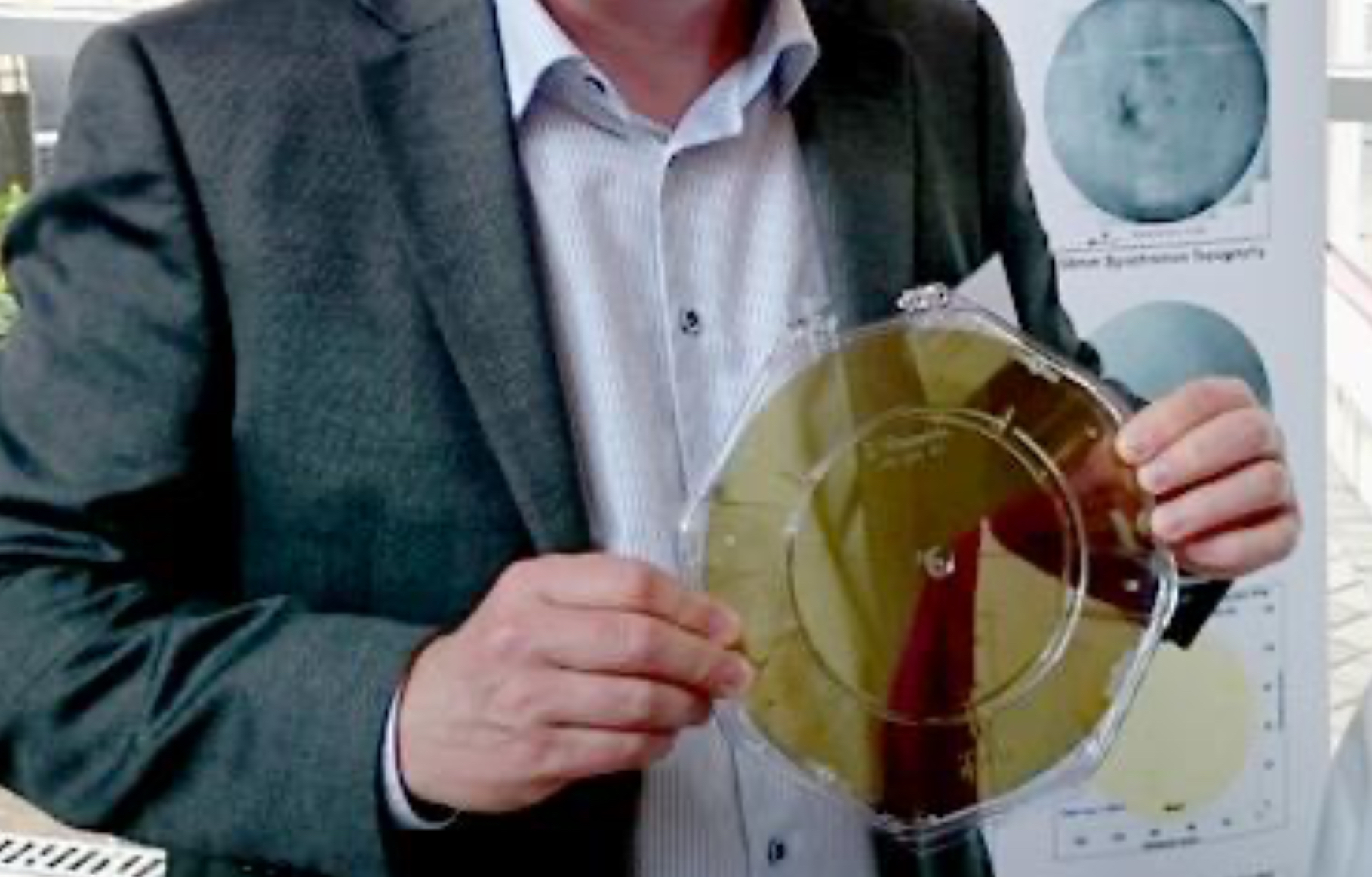
The CVD-systems are designed with Epiluvac ER3 reactors for 8-inch wafers epitaxy of SiC and GaN. They are intended to be used for R&D in new materials technology.
Roger Nilsson, Epiluvac’s CTO says: “The reactor development started years ago in cooperation with Linköping University. During the last years, we have refined the design into a brand-new platform. From the beginning, it is designed for 8- inch wafers that requires new solutions for controlling the temperature profile and gas flow concentration over the large wafer. It has also the unique feature that allows two or more systems to be put together to a WBG-Multi-Reactor-CVD-System. This multi-system approach allows the user to optimise the chemistry in each and every reactor, thereby achieving a very high yield.”
The systems are equipped with an automatic robotic wafer handler interfacing both reactors. To increase production capacity, the wafers are pre-heated and cooled down outside the reactor. Epiluvac offers a turnkey solution, including support to get the system up and running with basic epitaxial growth. The new ER3 also includes a patented feature where the wafer bow is minimised. Optionally, customers can add in-situ measurements for GaN.
Rolf Elmér, chairman of Epiluvac, adds: “There is a huge potential for sales of this new platform to the semiconductor industry. The new wide band-gap (WBG) semiconductor materials are used to produce more efficient power electronics devices. These devices are used in e.g. electrical vehicles, transformers for solar cells and smart micro power grids.


