
Los Alamos paves way to large-scale perovskite PV production
US team show how sulfolane-additive process yields easy fabrication, low cost, top performance, long operating life
A new, simpler solution process for fabricating stable perovskite solar cells overcomes the key bottleneck to large-scale production and commercialization of this promising renewable-energy technology, which has remained tantalisingly out of reach for more than a decade.
"Our work paves the way for low-cost, high-throughput commercial-scale production of large-scale solar modules in the near future," said Wanyi Nie, a research scientist fellow in the Center of Integrated Nanotechnologies at Los Alamos National Laboratory and corresponding author of the paper, which was published today in the journal Joule. "We were able to demonstrate the approach through two mini-modules that reached champion levels of converting sunlight to power with greatly extended operational lifetimes. Since this process is facile and low cost, we believe it can be easily adapted to scalable fabrication in industrial settings."
The team invented a one-step spin coating method using sulfolane ((CH₂)₄SO₂), a liquid solvent. The new process allowed the team, a collaboration among Los Alamos and researchers from National Taiwan University (NTU), to produce high-yield, large-area photovoltaic devices that are highly efficient in creating power from sunlight. These perovskite solar cells also have a long operational lifetime.
"We are excited about this achievement," said Prof. Leeyih Wang, the principal investigator of the NTU group and one of the corresponding authors, "this is a new synthetic route that is widely applicable in the rich perovskite material family." Hsin-Hsiang Huang, a graduate student at NTU and the first author of this paper, said, "We have implemented new chemistry to push it towards a technologically relevant demonstration."
Perovskite photovoltaics, seen as a viable competitor to the familiar silicon-based photovoltaics on the market for decades, have been a highly anticipated emerging technology over the last decade. Commercialisation has been stymied by the lack of a solution to the field's grand challenge: scaling up production of high-efficiency perovskite solar cell modules from the bench-top to the factory floor.
The research paper shows a new route to fabrication by introducing sulfolane as an additive in the perovskite precursor, or the liquid material that creates the perovskite crystal through a chemical reaction. As in other fabrication methods, that crystal is then deposited on a substrate.
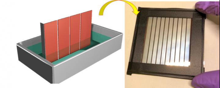
Through a simple dipping method, the team was able to deposit a uniform, high-quality perovskite crystalline thin film covering a large active area in two mini-modules, one of about 16 square centimetres and the other nearly 37 square centimetres. Fabricating uniform thin film across the entire photovoltaic module's area is essential to device performance.
The picture aboe shows the new dipping process.
For other perovskite fabrication methods, one of the major roadblocks to industrial-scale fabrication is their narrow processing window, the time during which the film can be laid down on the substrate. To get a uniform crystalline film that's well bonded to the layer below it, the deposition process has to be strictly controlled within a matter of seconds.
Using sulfolane in the perovskite precursor extends the processing window from 9 seconds to 90 seconds, forming highly crystalline, compact layers over a large area while being less dependent on the processing conditions.
The sulfolane method can be easily adapted to existing industrial fabrication techniques, which helps to pave the path toward commercialisation.
A perovskite is any material with a particular crystal structure similar to the mineral perovskite. Perovskites can be engineered and fabricated in extremely thin films, which makes them useful for solar photovoltaic cells.
'A simple one-step method with wide processing window' by Hsin-Hsiang Huang et al; Joule, March 18, 2021


