Mist-CVD enhances MIS-HEMTs

Thanks to mist CVD, pyrophoric materials and vacuum pumps are no longer needed to deposit insulators on GaN HEMTs
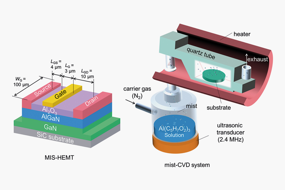
A Japanese collaboration is claiming to have produced the first metal-insulator-semiconductor (MIS) HEMTs with an alumina insulator added by mist-CVD, a cost-effective, environmentally friendly growth process.
This variant of the HEMT is less common than that with a Schottky gate, which has a simpler architecture, is easier to make, and produces a high transconductance. However, the Schottky gate HEMT dos have a drawback: it suffers from high leakage currents, originating from high input swings that drive the gate to forward bias. Addressing this issue is the MIS structure, formed by inserting an insulator between the AlGaN layer and the metal gate.
Unfortunately, the established deposition techniques for realising the MIS-HEMT requires the use of highly flammable toxic sources under vacuum. For example, the common approach to adding alumina (Al2O3) – an insulator with a high breakdown field and good permittivity – is atomic layer deposition, using trimethylaluminium, a highly pyrophoric material.
In comparison, the mist CVD technique pursued by the Japanese team – a partnership between researchers at the University of Fukui, Kwansei Gakuin University and Kumamoto University – is cost-effective and environmentally friendly, with deposition taking place at atmospheric pressure, so there is no need for energy-hungry vacuum pumps.
“On top of that, the mist CVD system employs far safer and cheaper aluminium acetylacetonate as the aluminium source,” says team spokesman Joel Asubar from the University of Fukui.
Asubar champions the simplicity of the technique, pointing out that a mist CVD system has just two major parts: an atomiser, which is very similar to a commercial ultrasonic humidifier; and a heater.
The challenge is to control the flow of the mist, which is part liquid, part gas. According to Asubar, it is knowledge of hydrodynamics and the pyrolysis reaction of the source precursor that has unlocked the “secret recipes” for depositing alumina over a semiconductor surface.
To demonstrate the capabilities of mist growth, the team compared the performance of devices produced by this approach with those incorporating a Schottky gate. Both types of transistor were fabricated from epiwafers featuring a SiC substrate and a 24 nm-thick AlGaN barrier – this ternary created a two-dimensional electron gas with a sheet carrier density of 1 x 1013 cm-2 and a mobility of 1510 cm2 V-1 s-1.
Fabrication of the HEMTs began by reactive-ion etching, which defined isolation trenches, and electron-beam evaporation that provided source and drain contacts. To make the MIS-HEMT, the team added Al2O3, using a mist created by dissolving aluminium acetylacetonate in methanol and atomising this liquid precursor with a 2.4 MHz ultrasonic transducer. Using a nitrogen carrier gas, it took just 90 s to deposit this film on a sample heated to 400degC,.
Merits of the MIS-HEMT made by mist CVD over that with a Schottky-gate have been demonstrated by measurements on devices with a 3µm long, 100µm wide gate and gate-to-drain and gate-to-source spacings of 10 µm and 4 µm respectively. Gate leakage current is three orders of magnitude lower, allowing the application of a +3V gate-source that boosts the maximum drain current to 780 mA mm-1. In addition, the reverse breakdown voltage higher – it is 320 V, compared with 210 V.
Asubra has also compared his MIS-HEMT made by mist CVD with the reports of MIS-HEMTs made by ALD that employ the same insulator. Those made by mist-CVD have an interface state density that tends to be lower and a subthreshold swing that is said to be “highly competitive”.
One of the collaboration’s next goals is to incorporate a high-speed, rotation-type mist-CVD system designed by Yusui Nakamura’s group at Kumamoto University. This tool has already realized highly uniform ZnO thin-films on 2-inch sapphire substrates.
Another plan is to build on recent work that uncovered an unexpectedly low level of fixed positive charges at mist-Al2O3/AlGaN interfaces.
“This means that it would be easier to obtain enhancement-mode devices using mist-Al2O3,” says Asubar, who intends to use this feature to obtain high-performance, safer ‘normally-off’ devices.
R. S. Low et al. Appl. Phys. Express 14 031004 (2021)


