Loading...
News Article

FBH invests in high-performance ion implantation

News

New tool allows for development of innovative planar integration processes in materials like GaN, AlN, and gallium oxide

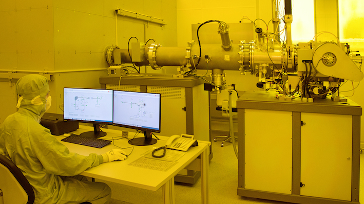
Berlin-based Ferdinand-Braun-Institut (FBH) has put a sophisticated ion implanter system from High Voltage Engineering Europa B.V. into operation.

The versatile tool will be used for developing innovative semiconductor devices, extending the technological capabilities of FBH for in-house research and customer processes. Among other things, the system enables doping implantations of wide-bandgap semiconductors.

The novel ion implanter offers high implantation currents of up to 2 mA and covers acceleration voltages from 5 keV to 500 keV. According to FBH, this allows materials to be systematically modified even at high implantation doses within industry-compatible process times. A sputtering source can also be used to implant materials with very high melting points, such as the special metals tungsten, molybdenum, tantalum, and niobium.

This opens up further technological possibilities. In addition to a gas source, the system is equipped with two furnaces to implant low melting metals. The new implanter offers another special feature: with a special sample holder, substrates can be heated up to 500degC. This enables activation of the dopants during implantation, for example in wide-gap semiconductors. The possibilities for selective isolation and doping make the new ion implanter an important technical foundation at FBH for the development of innovative planar integration processes in materials like GaN, AlN, and gallium oxide.

The procurement of the ion implanter and the required installation work in the cleanroom was funded by the Federal Ministry of Education and Research (BMBF) within the framework of Research Fab Microelectronics Germany (FMD) (funding reference 16FMD02).

SiC MOSFETs: Understanding the benefits of plasma nitridation
Wolfspeed reports Q2 results
VueReal secures $40.5m to scale MicroSolid printing
Mitsubishi joins Horizon Europe's FLAGCHIP project
Vishay launches new high voltage SiC diodes
UK team leads diamond-FET breakthrough
GaN adoption at tipping point, says Infineon
BluGlass files tuneable GaN laser patents
QD company Quantum Science expands into new facility
Innoscience files lawsuit against Infineon
Riber revenues up 5% to €41.2m
Forvia Hella to use CoolSiC for next generation charging
Photon Design to exhibit QD simulation tool
Ortel transfers CW laser fabrication to Canada
Luminus adds red and blue multi-mode Lasers
PseudolithIC raises $6M for heterogeneous chiplet tech
Mesa sidewall design improves HV DUV LEDs
IQE revenue to exceed expectations
'Game-changing' VCSEL system targets clinical imaging
German start-up secures finance for SiC processing tech
Macom signs preliminaries for CHIPS Act funding
IQE and Quintessent partner on QD lasers for AI
EU funds perovskite tandems for fuel-free space propulsion
EU to invest €3m in GeSi quantum project
Transforming the current density of AlN Schottky barrier diodes
Turbocharging the GaN MOSFET with a HfOâ‚‚ gate
Wolfspeed launches Gen 4 SiC MOSFET technology
Report predicts high growth for UK's North East
Element Six unveils Cu-diamond composite
SemiQ launches hi-rel 1700V SiC MOSFETs
Lynred to exhibit Eyesential SWIR sensor for machine vision
Thorlabs buys VCSEL firm Praevium Research
×
Search the news archive

To close this popup you can press escape or click the close icon.
Logo
x
Logo
×
Register - Step 1

You may choose to subscribe to the Compound Semiconductor Magazine, the Compound Semiconductor Newsletter, or both. You may also request additional information if required, before submitting your application.


Please subscribe me to:


You chose the industry type of "Other"

Please enter the industry that you work in: