Exposing the origins of substrate conduction within GaN-on-silicon HEMTs

Experiments uncover thermal donors and diffused group III elements as the causes of substrate conduction in GaN-on-silicon HEMTs
One of the biggest questions puzzling the nitride community concerns the origin of substrate conduction in GaN HEMTs. This mysterious malady saps away RF power, and understanding its cause could provide a crucial step in closing the performance gap between GaN-on-silicon HEMTs and those with a SiC foundation.
Shedding new insights on this matter is a UK collaboration between researchers at the University of Cambridge and Cardiff University.
Saptarsi Ghosh from the University of Cambridge told Compound Semiconductor that he and his co-workers have shown, for the first time, that the source of unintentional substrate conductivity for GaN-on-silicon stems from not one but two separate origins. There is an intrinsic contribution from thermal donors, as well as an extrinsic factor at play, group-III diffusion.
The team have shown that by carefully controlling the MOCVD growth process they can reduce the impact of this diffusion on device performance.
To fathom the causes of substrate conduction in RF GaN-on-silicon HEMTs the team carried out many experiments over about 18 months. “When we saw results that could not be explained by what was known, we had to plan new experiments to dig deeper.”
Investigations involved scrutinising a portfolio of home-grown samples, all produced on high-resistivity Czochralski-grown substrates. Float-zone high-resistivity wafers were ruled out for this study, due to their higher cost and propensity for plastic deformation.
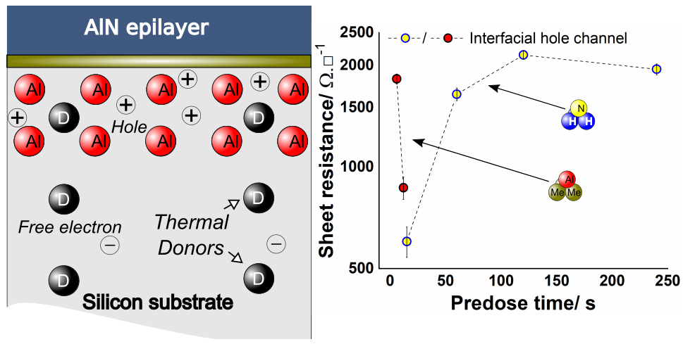
Two reference samples were included in the investigation – an unprocessed substrate, and another annealed at 1080 degC for 30 minutes. The team also employed this annealing step for the fabrication of six more samples, each with a 250 nm-thick AlN layer. Prior to the growth of this epilayers, the researchers treated the surface of the substrate with either an ammonia pre-dose for 15 s, 60 s, 120 s or 240 s, or a trimethylaluminium pre-dose for 6 s or 12 s.
Eddy current measurements revealed that annealing reduced the sheet-resistance from beyond the limit of the measurement system to 596 Ω/square, a fall of two orders of magnitude. By repeating these measurements after back-side thinning to eliminate any backside contamination, and probing the material with secondary-ion mass spectrometry and depth-dependent Hall measurements, the team pinpointed the cause of unintended conductivity: electrons distributed throughout the thickness of bulk silicon.
The team suspects that the most likely cause of this bulk conductivity is the generation of one or more thermally induced donors. Oxygen participates are viewed as a plausible candidate, due to the high-levels of intrinsic oxygen that are present in silicon substrates grown by the Czochralski process.
(Pictured above: substrate conduction comes from an n-type layer that is distributed throughout the substrate and has a purely thermal origin, and a p-type layer that is localised on the substrate side of the AlN-silicon interface and induced by group-III diffusion of the metal-organic precursor.)
Additional experiments by the team identified the second cause of substrate conduction: group-III acceptors that result in a p-type conductive layer at the AlN-silicon interface. The duration of the pre-dose with either ammonia or trimethylaluminium impacts sheet resistance. With a judicious choice, values as high as around 2000 Ω/square are possible.
The elemental diffusion that causes p-type conductivity may occur before, during or after the nucleation of AlN. Efficacy of the pre-dose is thought to be associated with inhibiting diffusion during the various stages of this nucleation process.
Ghosh and co-workers are planning to carry out electromagnetic simulations to correlate substrate conductivity with RF loss.“In parallel, we are planning growth experiments to figure out in which part of the aluminium growth step most of the diffusion occurs.”
'Origin(s) of Anomalous Substrate Conduction in MOVPE-Grown GaN HEMTs on Highly Resistive Silicon' by S. Ghosh et. al; ACS Appl. Electron. Mater. 3 813 (2021)


