
Changing 2D semiconductor symmetry can unlock its promise
Rensselaer group show how flexo-photovoltaic effect could be harnessed to design novel and/or high-efficiency optoelectronics
Optoelectronic materials that are capable of converting the energy of light into electricity, and electricity into light, have promising applications as light-emitting, energy-harvesting, and sensing technologies. However, devices made of these materials are often plagued by inefficiency, losing significant useful energy as heat. To break the current limits of efficiency, new principles of light-electricity conversion are needed.
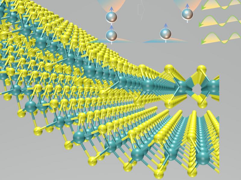
For instance, many materials that exhibit efficient optoelectronic properties are constrained by inversion symmetry, a physical property that limits engineers' control of electrons in the material and their options for designing novel or efficient devices. In research published in Nature Nanotechnology, a team of materials scientists and engineers, led by Jian Shi, an associate professor of materials science and engineering at Rensselaer Polytechnic Institute in the US, used a strain gradient in order to break that inversion symmetry, creating a novel optoelectronic phenomenon in the promising material MoS2 -- for the first time.
To break the inversion symmetry, the team placed a vanadium oxide (VO2) wire underneath a sheet of MoS2. MoS2 is flexible, Shi said, so it deformed its original shape to follow the curve of the VO2 wire, creating a gradient within its crystal lattice. Imagine what would happen if you placed a piece of paper over a pencil that was sitting on a table. The varied tension created in the paper is like the strain gradient formed in the MoS2 lattice.
That gradient, Shi said, breaks the material's inversion symmetry and allows electrons traveling within the crystal to be manipulated. The unique photo-response observed near the strain gradient allows a current to flow through the material. It's known as the flexo-photovoltaic effect, and it could be harnessed to design novel and/or high-efficiency optoelectronics.
"This is the first demonstration of such an effect in this material," Shi said. "If we have a solution that does not create heat during photon-electricity conversion, then the electronic devices or circuits could be improved."
VO2 is very sensitive to temperature, so the team was also able to demonstrate that the flexo-photovoltaic effect brought about temperature dependence at the site where the MoS2 and VO2 materials meet -- changing the lattice's gradient accordingly.
"This discovery suggests a novel principle that could be used for remote thermal sensing," said Jie Jiang, a postdoctoral research fellow in Shi's lab and the first author on this paper.
What the team was able to demonstrate here, Shi said, not only shows great promise for this material, but also suggests the potential of using such an approach in engineering other materials with favorable optoelectronic properties that are plagued by inversion symmetry.
'Flexo-photovoltaic effect in MoS2' by Jie Jiang et al; Nature Nanotechnology 17th June (2021)


