
Powder engineering could improve perovskite stability
Scientists from the Okinawa Institute turn their attention to perovskite solar cell absorber layer
In a new study, published in Nano Energy, researchers within the Energy Materials and Surface Sciences Unit, led by Yabing Qi, at the Okinawa Institute of Science and Technology Graduate University (OIST) have demonstrated that using a new method to create one of the raw materials necessary for perovskites could be key to the success of perovskite-based solar cells.
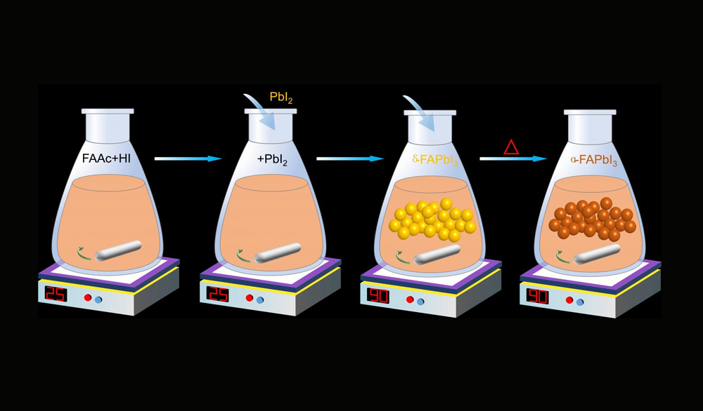
"There's a necessary crystalline powder in perovskites called FAPbI3, which forms the perovskite's absorber layer," explained one of the lead authors, Guoqing Tong, Postdoctoral Scholar in the Unit. "Previously, this layer was fabricated by combining two materials - PbI2 and FAI. The reaction that takes place produces FAPbI3. But this method is far from perfect. There are often leftovers of one or both of the original materials, which can impede the efficiency of the solar cell."
To get around this, the researchers synthesised the crystalline powder using a more precise powder engineering method. They still used one of the raw materials-PbI2-- but also included extra steps, which involved, amongst other things, heating the mixture to 90degC and carefully dissolving and filtering out any leftovers. This ensured that the resulting powder was high quality and structurally perfect.
Another benefit of this method was that the perovskite's stability increased across different temperatures. When the perovskite's absorber layer was formed from the original reaction, it was stable at high temperatures. However, at room temperature, it turned from brown to yellow, which wasn't ideal for absorbing light. The synthesised version was brown even at room temperature.
In the past, researchers have created a perovskite-based solar cell with more than 25 percent efficiency, which is comparable to silicon-based solar cells. But, to move these new solar cells beyond the lab, an upscale in size and long-term stability is necessary.
"Lab-scale solar cells are tiny," said Qi. "The size of each cell is only about 0.1 cm2. Most researchers focus on these because they're easier to create. But, in terms of applications, we need solar modules, which are much larger. The lifespan of the solar cells is also something we need to be mindful of. Although 25 percent efficiency has previously been achieved, the lifespan was, at most, a few thousand hours. After this, the cell's efficiency started to decline."
Using the synthesised crystalline perovskite powder, Tong, alongside Research Unit Technician Dae-Yong Son and the other scientists in Qi's Unit, achieved a conversion efficiency of over 23 percent in their solar cell, but the lifespan was more than 2000 hours. When they scaled up to solar modules of 5x5cm2, they still achieved over 14 percent efficiency. As a proof-of-concept, they fabricated a device that used a perovskite solar module to charge a lithium ion battery.
These results represent a crucial step towards efficient and stable perovskite-based solar cells and modules that could, one day, be used outside of the lab. "Our next step is to make a solar module that is 15x15cm2 and has an efficiency of more than 15 percent," said Tong. "One day I hope we can power a building at OIST with our solar modules."
'Removal of residual compositions by powder engineering for high efficiency formamidinium-based perovskite solar cells with operation lifetime over 2000 h' by GuoqingTong et al; Nano Energy 13 May 2021.


