
Swiss team adds superconducting contacts to 2D semiconductors
Combination could give rise to new quantum phenomena and find use in quantum technology, say University of Basel researchers
For the first time, University of Basel researchers have equipped the 2D compound semiconductor MoS2 with superconducting contacts. The researchers say that this combination could give rise to new quantum phenomena and find use in quantum technology.
Utrathin semiconductors promise to deliver unique characteristics that are otherwise very difficult to control, such as the use of electric fields to influence the magnetic moments of the electrons. In addition, complex quantum mechanical phenomena take place in these semiconducting monolayers that may have applications in quantum technology.
Scientists worldwide are investigating how these thin semiconductors can be stacked to form new synthetic materials, known as van der Waals heterostructures. However, until now, they have not succeeded in combining such a monolayer with superconducting contacts in order to dig deeper into the properties and peculiarities of the new materials.
Superconducting contacts
The team of physicists, led by Andreas Baumgartner in the research group of Christian Schönenberger at the Swiss Nanoscience Institute and the Department of Physics of the University of Basel, think components built on a combination of semiconductor and superconductor may exhibit new properties and physical phenomena.
"In a superconductor, the electrons arrange themselves into pairs, like partners in a dance - with weird and wonderful consequences, such as the flow of the electrical current without a resistance," explains Baumgartner, the project manager of the study. "In the semiconductor MoS2, on the other hand, the electrons perform a completely different dance, a strange solo routine that also incorporates their magnetic moments. Now we would like to find out which new and exotic dances the electrons agree upon if we combine these materials."
Suitable for use as a platform
The electrical measurements at the low temperatures required for superconductivity - just above absolute zero (-273.15degC) - show clearly the effects caused by the superconductor; for example, at certain energies, single electrons are no longer allowed. Moreover, the researchers found indications of a strong coupling between the semiconductor layer and the superconductor.
"Strong coupling is a key element in the new and exciting physical phenomena that we expect to see in such van der Waals heterostructures, but were never able to demonstrate," says Mehdi Ramezani, lead author of the study.
"And, of course, we always hope for new applications in electronics and quantum technology," says Baumgartner. "In principle, the vertical contacts we've developed for the semiconductor layers can be applied to a large number of semiconductors. Our measurements show that these hybrid monolayer semiconductor components are indeed possible -perhaps even with other, more exotic contact materials that would pave the way for further insights," he adds.
Fabrication process
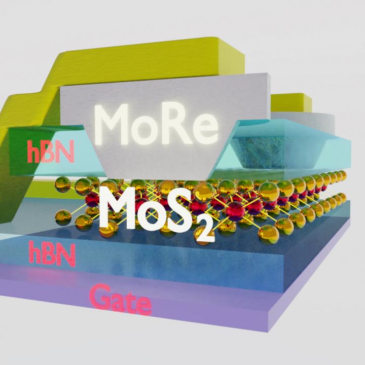
The fabrication of the new component in a type of sandwich made of different materials requires a large number of different steps. In each step, it is important to avoid contaminations, as they impair the transport of electrical charges.
To protect the semiconductor, the researchers pack a monolayer of MoS2 between two thin layers of boron nitride, through which they have previously etched the contacts vertically using electron-beam lithography and ion etching. They then deposit a thin layer of molybdenum rhenium as a contact material - a material that retains its superconducting properties even in the presence of strong magnetic fields.
Working under a protective nitrogen atmosphere in a glove box, the researchers stack the boron nitride layer onto the MoS2 layer and combine the underside with a further layer of boron nitride as well as a layer of graphene for electrical control. The researchers then place this elaborate van der Waals heterostructure on top of a silicon/silicon-dioxide wafer.
'Superconducting Contacts to a Monolayer Semiconductor' by Mehdi Ramezani et al; Nano Lett. June 23, 2021


