
ACM Launches Plating Tool for compound semis
Supports wafer-level packaging and plating applications in compound semiconductor manufacturing
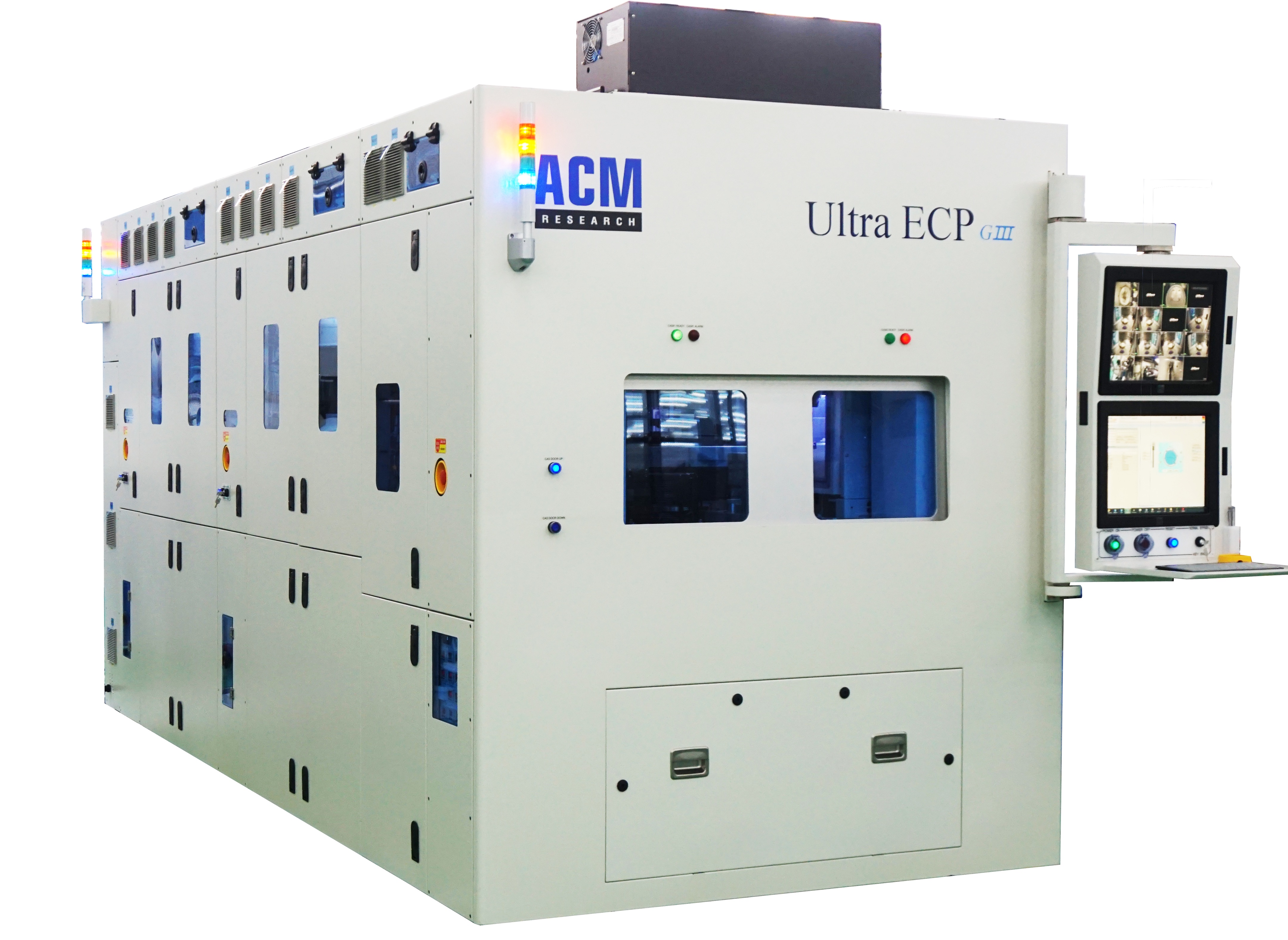
ACM Research, a supplier of wafer processing solutions, has announced the launch of its Ultra ECP GIII plating tool to support wafer level packaging for compound semiconductors, with product offerings for SiC, GaN and GaAs.
The tool is also capable of plating gold (Au) into backside deep hole processes with greater uniformity and better step coverage. The tool features a fully-automated platform to support high volume manufacturing that accommodates both flat and notched 6-inch wafers, and incorporates ACM’s proprietary second anode power and paddle technologies for optimal performance.
“The compound semiconductor market is growing rapidly with strong demand from electric vehicles, 5G communication, and RF and AI applications,” said David Wang, ACM’s CEO and president. “Historically, compound semiconductor manufacturing processes have seen limited levels of automation, and have been subject to restricted production volumes. Further, most plating has been performed by vertical-type plating tools with poor uniformity performance. ACM’s new Ultra ECP GIII plating tool overcomes these challenges to meet the growing volume and advanced performance demands for compound semiconductors.”
ACM says its Ultra ECP GIII tool leverages two key technologies to achieve performance benefits: ACM’s second anode and ACM’s paddle technology. ACM’s second anode technology delivers superior uniformity control by effectively tuning wafer-level plating performance to overcome issues created by electrical field distribution differences. It can be used to optimise big die at wafer edge area patterns and notch area to achieve plating uniformity within 3 percent.
ACM’s paddle technology achieves stronger agitation to enhance mass transfer, resulting in significantly better step coverage in deep holes. Improved step coverage enables a reduction in Au film thickness, achieving cost savings for the customer.
ACM has received two orders for the Ultra ECP GIII from China-based compound semiconductor manufacturers. The first order was delivered in July 2021 to support wafer level packaging with copper–nickel–tin-silver plating modules using second anode technology, and was integrated with a vacuum pre-wet chamber and a post-clean chamber. The second order, scheduled to be delivered later in the quarter ending September 30, 2021, is for a gold (Au) plating system.


