
Enkris demonstrates 300mm GaN-on-Si HEMT wafers
Epiwafers show uniformity and low wafer bow for 200V, 650V and 1200V power applications
Enkris Semiconductor, a GaN wafer epi-foundry based at Suzhou Industrial Park, China, has announced that it has demonstrated a series of high-quality 300mm GaN-on-Si HEMT epiwafers of good thickness uniformity and low wafer bow for 200V, 650V and 1200V power applications – paving the way for device processing using more sophisticated 300mm CMOS-compatible lines.
Commercial GaN power devices based on GaN-on-Si HEMT technology are gaining in popularity for a wide range of applications such as consumer electronics, industrial electronics and data centres, and in the energy, automotive and mobility sectors. Driven by cost reduction and more sophisticated integrated circuit design, the industry is now moving towards larger wafer sizes.
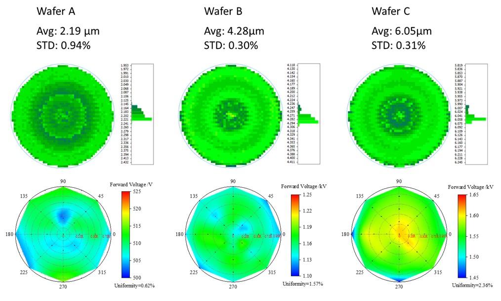
Following its successful launch of commercial 200mm GaN-on-Si HV HEMT epiwafers in 2014, Enkris Semiconductor has now successfully transferred its AlGaN/GaN HEMT epitaxy process to 300mm Si substrates, while maintaining the excellent thickness uniformity and low wafer bow within 50µm. The vertical voltage breakdown measurements suggest the wafers are suitable for 200V, 650V and 1200V power applications (figure 1, top of page).

The 300mm GaN-on-Si HEMT epitaxial layer structure adopted to solve the key issues of wafer cracking/bow and high crystalline defects is shown above in figure 2(a). The growth starts with an AlN nucleation layer, followed by a strain relief stack, GaN channel, AlGaN barrier and GaN cap. The narrow XRD AlN(002) peak and a good uniformity of FWHM, as shown above in figure 2(b), indicate a high crystalline quality across the whole 300mm wafer.

Figure 3 (above) shows the Al composition in the AlGaN barrier and the 2DEG carrier concentration measured at nine positions from wafer centre to wafer edge. The measurements give an average value of 19.9 percent and a std of 0.68 percent of Al composition in the AlGaN barrier (figure 3a), suggesting a uniform 2DEG electrical characteristics. This has been confirmed by the CV measurements, revealing an average electron concentration of 7.2E12 cm-2 with a std <2 percent (figure 3b).
“Thanks to our optimised AlN nucleation layer, we are able to produce crack-free GaN-based HEMT epiwafers that meet the leakage current requirements on large size Si substrates up to 300mm,” sai Kai Cheng, CEO of Enkris. “Despite the challenges in the epitaxy process, strain management and defect control when moving to 300mm wafer size, we have achieved excellent structural quality and electrical properties in the AlGaN/GaN HEMT structures. This will certainly encourage the development of high-power integrated circuits to yield system-on-chip and further reduce the cost of GaN power devices.”


