
Could new technique pave way to perfect perovskites?
Next-gen solar material could outshine other solar cells
Perovskites are promising active layers in photovoltaics and other types of electronic devices that respond to or control light including LEDs, detectors, and lasers.
But although perovskites offer great potential for greatly expanding solar power, they have yet to be commercialised because their reliable synthesis and long-term stability has long challenged scientists, explains Carolin Sutter-Fella, a scientist at the Molecular Foundry, a nanoscience user facility at Lawrence Berkeley National Laboratory (Berkeley Lab). Now, a path to perfect perovskites may soon be within reach.
A recent Nature Communications study co-led by Sutter-Fella reports that solar materials manufacturing could be aided by a sophisticated new instrument that uses two types of light – invisible X-ray light and visible laser light – to probe a perovskite material’s crystal structure and optical properties as it is synthesised.
“When people make solar thin films, they typically have a dedicated synthesis lab and need to go to another lab to characterise it. With our development, you can fully synthesise and characterise a material at the same time, at the same place,” she said.
For this work, Sutter-Fella assembled an international team of top scientists and engineers to equip an X-ray beamline endstation with a laser at Berkeley Lab’s Advanced Light Source (ALS).
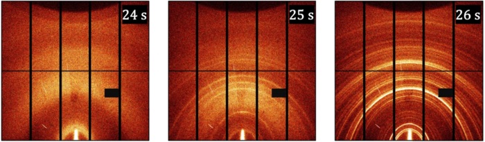
The new instrument’s highly intense X-ray light allows researchers to probe the perovskite material’s crystal structure and unveil details about fast chemical processes. For example, it can be used to characterise what happens in the second before and after a drop of a solidifying agent transforms a liquid precursor solution into a solid thin film. (The pic above shows what happens (from left to right) in the second before, during, and after a drop of a solidifying agent transforms a liquid precursor solution into a perovskite solar material.)
“Equipping an X-ray beamline endstation with a laser empowers users to probe these complementary properties simultaneously,” explained Sutter-Fella.
This combination of simultaneous measurements could become part of an automated workflow to monitor the production of perovskites and other functional materials in real time for process and quality control.
Perovskite films are typically made by spin coating, an affordable technique that doesn’t require expensive equipment or complicated chemical setups. And the case for perovskites gets even brighter when you consider how energy-intensive it is just to manufacture silicon into a solar device – silicon requires a processing temperature of about 2,732 degrees Fahrenheit. In contrast, perovskites are easily processed from solution at room temperature to just 302 degrees Fahrenheit.
The beamline endstation allows researchers to observe what happens during synthesis, and in particular during the first few seconds of spin coating, a critical time window during which the precursor solution slowly begins to solidify into a thin film.
First author Shambhavi Pratap, who specialises in the use of X-rays to study thin-film solar energy materials, played a critical role in developing the instrument as an ALS doctoral fellow. She recently completed her doctoral studies in the Müller-Buschbaum group at the Technical University of Munich.
“The instrument will allow researchers to document how small things that are usually taken for granted can have a big impact on material quality and performance,” Pratap said.
“To make reproducible and efficient solar cells at low cost, everything matters,” Sutter-Fella said. She added that the study was a team effort that spanned a wide range of scientific disciplines.
The work is the latest chapter in a body of work for which Sutter-Fella was awarded a Berkeley Lab Early Career Laboratory Directed Research and Development (LDRD) Award in 2017.


