
Cameca adds to Atom Probe Tomography range
Invizo 6000 and the LEAP 6000 XR advance the APT approach in academic labs and manufacturing facilities
Cameca, a business unit of Amatek, has announced two new atom probe tomography platforms, the Invizo 6000 and the LEAP 6000 XR, developed at the Atom Probe Technology Center in Madison, Wisconsin.
Atom Probe Tomography (APT) is a material science method enabling 3D nanoscale compositional characterisation of metals and alloys, ceramics, semiconductors, biomaterials, and geological materials.
“Since developing the revolutionary Local Electrode Atom Probe, Cameca has remained at the forefront of APT instrument design,” said Jesse Olson, Cameca business unit manager. “Major new features of the Invizo 6000 and LEAP 6000 XR atom probes promise to further advance this research technique in both academic laboratories and manufacturing facilities worldwide.”
The newest addition to the instrument line, the Invizo 6000, incorporates patented electrostatics that enable an increased field of view; a deep ultraviolet (DUV) laser module; advanced beam delivery optics that allow for dual-side specimen laser illumination; and a new extraction electrode design. The Invizo 6000 provides increased analysis volumes to capture larger features of interest and improves analytical measurements for a diverse set of applications, such as metallurgy, geoscience, batteries, and semiconductors.
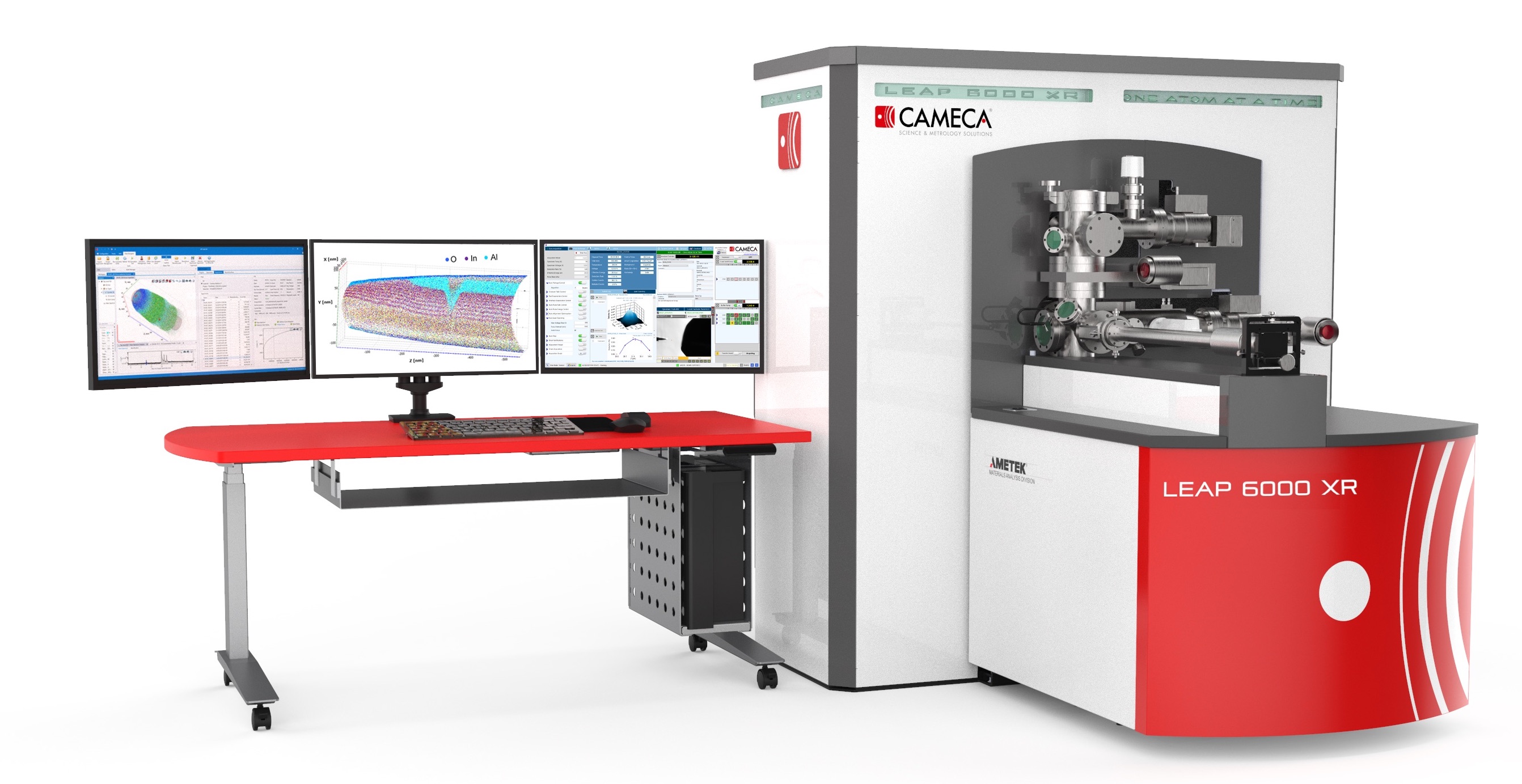
The latest instrument in the LEAP line of atom probes, the LEAP 6000 XR, builds on the proven utility of the LEAP platform. It delivers analytical accuracy and precision while maintaining the microtip compatibility and automation required to support a high sample volume environment. Specimen throughput and ease-of-use are enhanced by the automation of laser-specimen-electrode alignment, and the 6000 XR adds DUV laser pulsing to deliver improvements in both data quality and specimen yield. Furthermore, it introduces a novel simultaneous voltage-laser pulsing mode to increase detection sensitivity by an order of magnitude to enhance applications in semiconductors and other materials.


