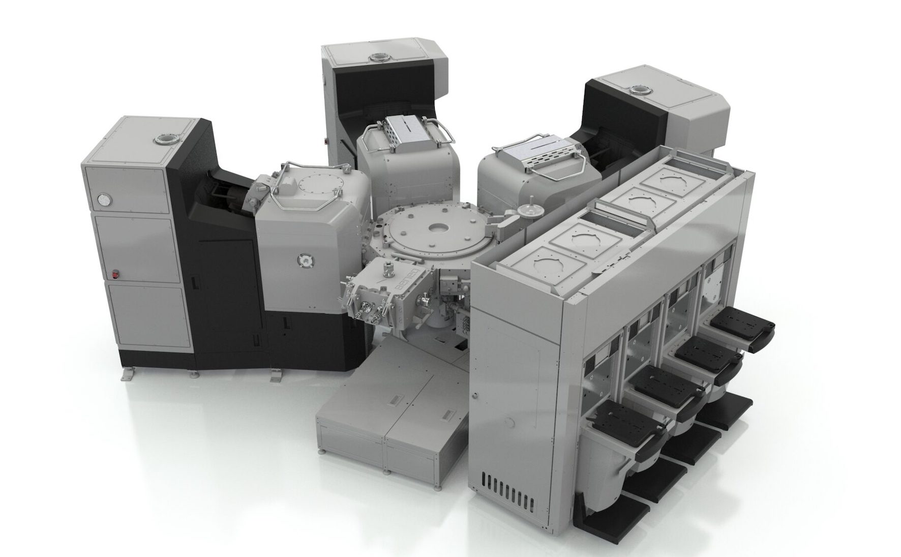
Beneq unveils two new ALD products

Transform 300 and Prodigy tools designed to meet needs for versaility and simplicity
Beneq, a forerunner in industrial production using atomic layer deposition (ALD), has launched two new products for semiconductor device fabrication: the Transform 300 and Prodigy.
The Beneq Transform 300 and Prodigy were each designed in response to growing technology requirements in the semiconductor manufacturing sector.
“The Transform 300 is designed to meet the growing demand of emerging semiconductor applications at 300 mm for devices such as CMOS image sensors, power devices, micro-OLED/LED, and advanced packaging, which call for a high degree of versatility,” explains Patrick Rabinzohn, VP, Semiconductor ALD at Beneq.
“We created Prodigy to address those market segments that need a simple solution supported by high-end technology. It inherits the ALD design and processing knowhow we at Beneq have developed over the last 15 years, packing advanced features in a simpler, targeted industrial form factor,” continues Rabinzohn.
Beneq Transform 300 (pictured above) is claimed to be the only 300 mm ALD cluster tool that combines thermal ALD (batch) and plasma ALD (single wafer) technologies to provide a versatile platform for IDMs and foundries. It is dedicated to advanced thin-film applications in CIS, Power, Micro-OLED/LED, Advanced Packaging and other MtM applications.
Beneq Tranform 300 is designed to cater to multiple advanced thin-film applications ranging from gate dielectric including in high aspect ratio trenches, to anti-reflection coating, final passivation or encapsulation, Chip-Scale-Packaging and beyond.
The Beneq Prodigy is designed for manufacturing compound semiconductors including RF IC’s (GaAs/GaN/InP), LED, VCSEL, Light Detectors and for MEMS manufacturers and foundries looking to enhance device performance and reliability through an affordable stand-alone ALD batch tool. Beneq Prodigy provides passivation and encapsulation films across multiple wafer types and sizes.


