Loading...
News Article

Samco Unveils New Plasma Etching Cluster Tool

News

'Cluster H' tool provides full-scale production capabilities for compound semiconductor devices

Samco, a manufacturer of etching, deposition and surface treatment processing equipment, has introduced the new plasma etching cluster tool Cluster H.

“With our cutting-edge plasma etching technology, Cluster H provides full-scale production capabilities for compound semiconductor devices such as high-frequency filters, SiC/GaN power devices, GaAs VCSELs, micro-OLED/LED, CMOS image sensors, and advanced packaging,” explains Tsukasa Kawabe, president and COO of Samco.

“We created Cluster H to meet the strong demand from our valued customers for high throughput equipment. Cluster H with etching processes available only at Samco enables the combination of optimal materials and process technologies in advanced electronic device fabrication,” continues Tsukasa.

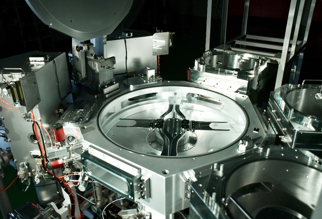
Cluster H is a cluster tool for etching and ashing that supports direct transfer of 6 inch and 8 inch diameter wafers. Centred on a hexagonal vacuum transfer platform, it is equipped with two vacuum cassette chambers and one vacuum aligner as part of the standard equipment configuration, and up to three process modules that can be attached.

The ICP etching process module uses the reaction chamber of the high-end ICP etching model RIE-800iP and is backed by our extensive process library and best-known methods. In addition, the frog-leg dual-blade robot enables high wafer throughput, compact transfer chamber, and system footprint.

In addition, the revamped software incorporates useful functions with improved reliability. The standard system is equipped with a user-friendly GUI and equipment management functions such as equipment performance tracking, wafer transfer history for each module and packages, and simulation functions for higher-level communication, and supports the manufacturing execution system (MES) used at customers’ factories.

SiC MOSFETs: Understanding the benefits of plasma nitridation
Wolfspeed reports Q2 results
VueReal secures $40.5m to scale MicroSolid printing
Mitsubishi joins Horizon Europe's FLAGCHIP project
Vishay launches new high voltage SiC diodes
UK team leads diamond-FET breakthrough
GaN adoption at tipping point, says Infineon
BluGlass files tuneable GaN laser patents
QD company Quantum Science expands into new facility
Innoscience files lawsuit against Infineon
Riber revenues up 5% to €41.2m
Forvia Hella to use CoolSiC for next generation charging
Photon Design to exhibit QD simulation tool
Ortel transfers CW laser fabrication to Canada
Luminus adds red and blue multi-mode Lasers
PseudolithIC raises $6M for heterogeneous chiplet tech
Mesa sidewall design improves HV DUV LEDs
IQE revenue to exceed expectations
'Game-changing' VCSEL system targets clinical imaging
German start-up secures finance for SiC processing tech
Macom signs preliminaries for CHIPS Act funding
IQE and Quintessent partner on QD lasers for AI
EU funds perovskite tandems for fuel-free space propulsion
EU to invest €3m in GeSi quantum project
Transforming the current density of AlN Schottky barrier diodes
Turbocharging the GaN MOSFET with a HfO₂ gate
Wolfspeed launches Gen 4 SiC MOSFET technology
Report predicts high growth for UK's North East
Element Six unveils Cu-diamond composite
SemiQ launches hi-rel 1700V SiC MOSFETs
Lynred to exhibit Eyesential SWIR sensor for machine vision
Thorlabs buys VCSEL firm Praevium Research
×
Search the news archive

To close this popup you can press escape or click the close icon.
Logo
x
Logo
×
Register - Step 1

You may choose to subscribe to the Compound Semiconductor Magazine, the Compound Semiconductor Newsletter, or both. You may also request additional information if required, before submitting your application.


Please subscribe me to:


You chose the industry type of "Other"

Please enter the industry that you work in: