Loading...
News Article

Samco Opens new Research Centre

News

Kyoto-based centre to focus on development of thin film deposition systems and process technologies, as well as basic research on thin film properties

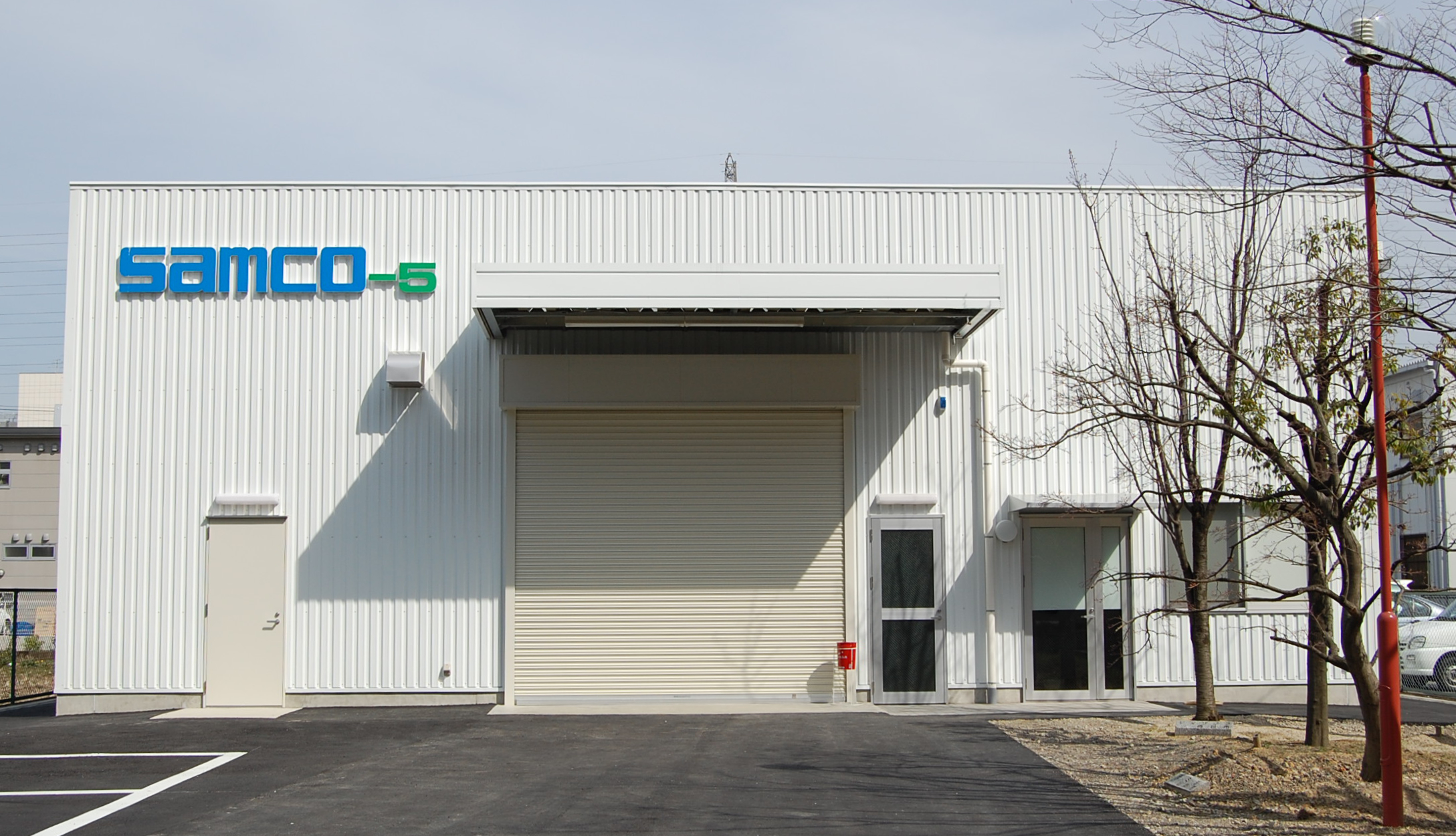
Samco, a manufacturer of etching, deposition and surface treatment processing equipment, has opened a new Research Centre for Nano Thin Films & Materials for ALD and mist CVD process and system development in Kyoto, Japan.

In recent years, the demand for ALD systems has been expanding for semiconductor and electronic device applications, and new markets are emerging in medical and healthcare fields such as coating technology for containers and medical devices. To meet growing market needs and with the aim of entering new markets in the future, Samco reorganised its former Basic Technology Research Centre and established the Research Center for Nano Thin Films & Materials. It has a building area of 413.90 m2 and is equipped with deposition systems for demonstrations and various measurement tools for evaluation.

“The Research Centre focuses on the development of thin film deposition systems and process technologies, as well as basic research on thin film properties and physical properties evaluation,” said Osamu Tsuji, the founder and CEO of Samco Inc. “We already have an extensive track record with ALD equipment, which we began selling in 2015 in the fields of semiconductor and electronic devices. Our next plan is to develop new ALD systems for medical and healthcare applications such as barrier films, coating films, medical materials, and coating of implant materials.”

Samco plans to increase its number of researchers at the Research Centre from the current 8 to 20 in the next 3 years and to expand its annual ALD systems sales to 3 billion yen in five years.

Mitsubishi joins Horizon Europe's FLAGCHIP project
Vishay launches new high voltage SiC diodes
UK team leads diamond-FET breakthrough
GaN adoption at tipping point, says Infineon
BluGlass files tuneable GaN laser patents
QD company Quantum Science expands into new facility
Innoscience files lawsuit against Infineon
Riber revenues up 5% to €41.2m
Forvia Hella to use CoolSiC for next generation charging
Photon Design to exhibit QD simulation tool
Ortel transfers CW laser fabrication to Canada
Luminus adds red and blue multi-mode Lasers
PseudolithIC raises $6M for heterogeneous chiplet tech
Mesa sidewall design improves HV DUV LEDs
IQE revenue to exceed expectations
'Game-changing' VCSEL system targets clinical imaging
German start-up secures finance for SiC processing tech
Macom signs preliminaries for CHIPS Act funding
IQE and Quintessent partner on QD lasers for AI
EU funds perovskite tandems for fuel-free space propulsion
EU to invest €3m in GeSi quantum project
Transforming the current density of AlN Schottky barrier diodes
Turbocharging the GaN MOSFET with a HfO₂ gate
Wolfspeed launches Gen 4 SiC MOSFET technology
Report predicts high growth for UK's North East
Element Six unveils Cu-diamond composite
SemiQ launches hi-rel 1700V SiC MOSFETs
Lynred to exhibit Eyesential SWIR sensor for machine vision
Thorlabs buys VCSEL firm Praevium Research
Advancing tuneable InP lasers on a heterogeneous platform
P-GaN gate HEMTs have record threshold voltage
Guerrilla RF releases GaN power amplifier dice
×
Search the news archive

To close this popup you can press escape or click the close icon.
Logo
x
Logo
×
Register - Step 1

You may choose to subscribe to the Compound Semiconductor Magazine, the Compound Semiconductor Newsletter, or both. You may also request additional information if required, before submitting your application.


Please subscribe me to:


You chose the industry type of "Other"

Please enter the industry that you work in: