UCLA team makes bioelectronic membranes from MoS2

2D compound semionductor could lead to new classes of wearable devices, diagnostic sensors and biological-electronic hybrid organisms
UCLA researchers have developed a unique design of ultrathin MoS2 films for highly flexible yet mechanically robust bioelectronic membranes that could pave the way for diagnostic on-skin sensors that fit precisely over the body’s contours and conform to its movements.
Science recently published a paper describing the research co-led by Xiangfeng Duan, professor of chemistry and biochemistry; and Yu Huang, professor and chair of the Materials Science and Engineering Department at the UCLA Samueli School of Engineering.
The ultrathin electronic membranes are made of several layers of atomically thin sheets of the inorganic compound MoS2. Each sheet is only two to three nanometers thick.
The key to maintaining the membrane’s structural integrity while keeping it thin lies in its layered patchwork structure. The layers are not a single continuous sheet but instead are an assemblage of smaller pieces. The layers are loosely connected by nonbonding van der Waals forces. This allows the sheets to independently slide and rotate over one another, creating extraordinary pliability while keeping their electronic functionality intact.
The layered patchwork creates a percolating network of nanochannels, large enough for air and water molecules to pass through them, giving the material its permeability and breathability.
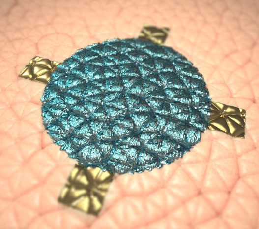
The researchers think that further development of this material could lead to noninvasive electronics for medicine, health care, biology, agriculture and horticulture. The researchers named the material van der Waals thin film, or VDWTF. The picture above shows an artistic representation of a skin transistor made from van der Waals thin films.
“Conceptually, the membrane is like a much-thinner version of kitchen cling film, with excellent semiconducting electronic functionality and unusual stretchability that naturally adapts to soft biological tissues with highly conformal interfaces,” Duan said. “It could open up a diverse range of powerful sensing and signaling applications. For example, wearable health-monitoring devices built with this material can accurately track electrophysiological signals at the organism level or down to the level of individual cells.”
The researchers created several demonstrations using the thin films, including a transistor that sat on top of a succulent plant’s leaf, whose abundant electrolytes were used to create the electronic circuit. They also created a similar transistor for human skin that used electrolytes-present skin cells to complete the circuit. In addition, the team developed an electrocardiogram that uses small circles of the film placed on a person’s right and left forearm and could detect their blinking during meditation.
“Our proof-of-concept demonstrations using the van der Waals thin film really just hint at the myriad possibilities for this new material,” Huang said. “The membrane could serve as the connection for human-machine interfaces, enhanced robotics and artificial intelligence-enabled technologies that connect directly. This could open a pathway to synthetic electronic-cellular hybrids — cyborg-like living organisms with electronic enhancements.”
'Highly stretchable van der Waals thin films for adaptable and breathable electronic membranes'; Science 24 Feb 2022


