Toyoda Gosei makes GaN Substrates over 6 inches

Project with Osaka University increases diameter of GaN substrates to over 6 inches
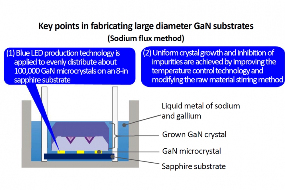
In a project headed by the Japanese Ministry of the Environment, Toyoda Gosei and Osaka University have fabricated a high quality GaN substrate (GaN seed crystal) of over 6 inches.
With help from Toyoda Gosei's expertise in GaN semiconductors (blue LEDs and UV-C LEDs), they used a method of growing GaN crystals in liquid metal of sodium and gallium (sodium flux method).
They will next conduct quality assessments for mass production of 6-inch substrates, and continue improving quality and increasing diameter size (more than 6 inches).
The technology innovation is part of a large project that includes verification of CO2 reductions from social implementation of applied products based on the development of GaN substrates.


