
A debut for AlPN
When grown on GaN, AlPN creates a strong polarization that promises to enhance the performance of the high-frequency HEMT
BY MARKUS PROSTOVEK FROM NAGOYA UNIVERSITY
MOST OF US have never encountered a new material. While it’s certainly not unusual to change from one material system to another during a career – migrating from classical III-Vs to the III-nitrides is a well-trodden pathway – it is rare to be there first. Even in academia, which fosters a more adventurous outlook than industry, incremental improvements are the norm, with research tending to be driven by opportunities identified within new applications.
This state of affairs is particular true in the III-Nitrides. In addition to AlN and GaN, just three ternaries are used for all devices – AlGaN, InGaN, and AlInN – with the latter of these rarely employed. Using ternaries brings challenges, primarily strain, with only Al0.83In0.17N offering lattice-matching to GaN. In sharp contrast, it is relatively easy to realise lattice matching with the more traditional III-Vs. Best known is the pairing of GaAs and AlGaAs, which unite to make the highly reflective mirrors of a VCSEL; but don’t forget the great versatility of InGaAsP, which offers compositions that can be lattice-matched to GaAs or InP while realising bandgap engineering.
Several attempts have been made to broaden the III-nitrides material portfolio. A pre-requisite for any such effort is a suitable metal-organic precursor, since all commercial growth uses MOCVD.

Figure 1. Calculated X-ray diffraction around (0002) GaN for HEMT
structures on GaN with different materials, assuming 106 counts/s for
GaN (0002).
BGaN has been tried out for some time, since there are available precursors – even if their primary purpose is rocket fuel! However, research has revealed that the (hypothetical) wurtzite BN has an even lower bandgap than AlN, and also higher strain. What’s more, it is challenging to incorporate more than a few percent boron, making the established wide bandgap ternary, AlGaN, superior in almost all respects.
More recently, attempts have been made to alloy scandium to form AlScN-on-GaN, a promising combination for realizing high polarization in an RF HEMT. Using MBE, researchers have grown layers of wurtzite AlScN that are stable for a scandium content up to 50 percent. Replicating these results in MOCVD has been very challenging, because metal-organic scandium-based precursors have a very low vapour pressure. There are also concerns over purity, although it is improving.
Arsenides and phosphides
If the starting point to develop a new material is a proven metal-organic precursor, then deciding to incorporate either arsenic or phosphorous is a logical way forward. After all, both are used a lot in classical III-Vs.
Some effort has already been devoted to alloying arsenic into GaN. The problem is that as arsenic is an even larger atom than gallium, it cannot squeeze into the tiny space of a nitrogen-lattice site. Due to this, in wurtzite GaAsN almost more arsenic goes on a gallium lattice site than there is on an nitrogen lattice site. Another impediment to the growth of GaAsN is that there is a low bond energy for an arsenic atom on a nitrogen site, causing arsenic to mostly desorb at the high growth temperatures required for epitaxy.
This leaves phosphorous. With a covalent radius between gallium or aluminium and nitrogen, it should be a little easier to incorporate phosphorous than arsenic on a nitrogen-lattice site.
Between 1996 and 2006, researchers tried to develop the growth of wurzite GaPyN1-y on GaN. This effort delivered limited success, realising homogenous layers with a phosphorous-content up to 3 percent. However, when attempts were made to produce films more rich in phosphorous, this lead to the formation of two classes of imperfection: phosphorous-antisites, that is phosphorous atoms located where gallium atoms should be; and PxNx clusters, attributed to both the shorter bond length of P-N than Ga-N and the larger size of phosphorous than nitrogen. These defects are driven by strain: when GaPN is grown on GaN this ternary is compressively strained, so the presence of phosphor on a gallium site can reduce this strain. This inherent limitation put an end to research on GaPN.
What about AlPN on GaN? This has much promise: AlN is tensile strained on GaN, so beyond the valences, phosphorous atoms have a further incentive to stay on the group V site. Note that this is not a new idea. Back in 1999 a team at Panasonic filed a patent associated with the strain relaxation potential, proposing AlGaNP instead of AlGaN. However, no experimental results were ever published.
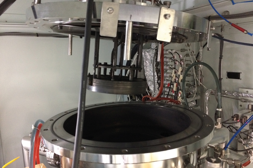
Since 2012 I have been keen to investigate the prospects of AlPN on GaN. I didn’t get the chance to pursue this when working as a postdoc, but when I took up the position of a Designated Professor at Nagoya University in 2017 the situation changed and I finally got to the chance to try and grow this new ternary, using a closed coupled showerhead reactor made by EpiQuest.
One obvious candidate for the source of phosphorous is PH3. For us, however, phosphine is not an option, due to its toxicity that prevents its use in our lab – but that’s not a disaster, as even if our team had been granted permission, it’s not trivial for us to use this source, as it would demand new bottle cabinets, security electronics and scrubbing systems. Instead we’ve turned to the liquid precursor tertiary butylphosphine (tBP). This is a move that has taken me full circle, as I helped to evaluate this less toxic phosphor precursor during my diploma thesis. (In the run up to the turn of the century tBP was developed to a high standard, when California thought about banning the use of PH3.) We started by hooking up the tBP bubbler to a repurposed MO line.

Figure 2. X-ray diffraction from multiple AlPN/GaN quantum wells with increasing tBP partial pressure grown at 1100°C.
Getting going
Uncovering suitable growth conditions is the first task when trying to grow any new material. Luckily, for AlPN we did not have to start from scratch, as we could draw on what’s been accomplished for AlN, which is closer to AlP than you may think.
These efforts have been aided by access to a handful of reports on the growth of cubic AlP, as well as my own attempts at trying to grow this material ten years ago. All those efforts involved cranking up the temperature of the reactor to its maximum – so between 750 °C and 950 °C – and employing relatively low V/III ratios, in the range 20-100. These conditions are similar to those for AlN growth, which again uses as high a temperature as possible – in this case between 1150 °C and 1250 °C – and V/III ratios of 50-100.
For our starting point we chose 1100 °C, a half-way house that still allows the growth of good GaN. We also selected a low V/III ratio. This is not only an obvious choice, based on the conditions used for the growth of AlP and AlN, but helps to reduce the impact of contamination and trim development costs, because tBP is relatively expensive compared with NH3 and PH3.
Realising success is not easy, due to the huge lattice mismatch between GaN and AlN. This causes all high-aluminium-content ternaries, including AlGaN, AlInN and AlPN, to easily crack on GaN after film growth exceeds just a few nanometres. While it is possible to grow very thin layers, it is challenging to characterise them with the most common technique used for analysing material composition and quality, X-ray diffraction. Efforts are hampered by the low values for the total number of electrons in aluminium, phosphorous and nitrogen, causing these atoms to be weak X-ray scatterers. For AlPN of similar thickness to AlGaN, the signal produced in X-ray diffraction is ten times lower (see Figure 1). Another impediment to progress with very thin films of AlPN is that due to the much higher partial pressures of group V-precursors needed for growth, there is the threat that the interface will be less abrupt, due to hetero-exchange reactions. Another challenge to prevent is a nitrogen-rich surface layer forming during cooling.
Given these difficulties, it’s of no surprise that the X-ray diffraction spectra for our first superlattices showed relatively broad peaks and an absence of clear Pendellösung. Still, we were able to use the zero-order peaks to calculate the phosphorous content. For this, we had the good fortune of being able to draw on the calculation of lattice constants and elastic constants for wurtzite AlP (and many other materials), undertaken in The Materials Project. When carrying out our X-ray calculations, we used corrected versions of calculated lattice constants, adjusted using the same factor needed to match the calculated lattice constants of AlN to their experimental values.
Assuming a similar growth rate to that of GaN for thick layers, we estimated X-ray spectra for AlPN-based superlattices with a phosphorous content up to 10 percent. When the phosphorous content exceeded this figure, we found that the features in the X-ray spectra associated with the quantum wells completely vanished, to leave just a broad shoulder (see Figure 2).
This observation is consistent with our hypothesis that tensile strain is critical: at a concentration of 11 percent the AlPN layer becomes compressively strained, with excess phosphorous forming black adsorbing PxNx clusters. It’s the same state of affairs when an AlPN layer cracks. The relaxed (cracked) AlPN has less than 3 percent AlPN, with excess phosphorous forming inclusions. It is clear that the key to growing AlPN with a higher phosphorous content is to avoid compressive strain or relaxation.
The good news is that when it comes to fabricating a HEMT, a thin layer suffices. For high-frequency HEMTs, what matters most is as high a polarization as possible. Currently AlInN provides this, while AlScN, under research, could yield far higher polarization charges (see Figure 3). However, growing AlScN by MOCVD is very challenging. AlPN has much promise, with a composition of AlP0.05N0.95 offering a similar degree of polarization to AlScN. Thanks to strong impact on the lattice constants of even a low phosphorous content, the critical thickness for this ternary is in excess of 20 nm.
This work, still in its infancy, is producing very encouraging results. We have fabricated structures with sheet resistances below 200 Ω/squ. and conducted low-temperature Hall measurements that have uncovered a two-dimensional electron gas.
An open question is the optical properties of AlPN. To ensure high-quality, this layer must be thin. We have found that when the thickness is below 60 nm, carriers drift into the neighbouring smaller bandgap GaN layers, where recombination takes place. So the unambigeous confirmation of the band gap bowing is still in the long homework list for this material.

Figure 3. Calculated sheet carrier density in HEMT structures using
different barrier materials. Adapted from T. Kazior et al. 2019
IEEE/MTT-S International Microwave Symposium. The curve for AlPN has
been added assuming that the polarisation coefficients of AlP0.1N0.9 are
similar to Al0.9Ga0.1N.
Reactor modifications
Our success has been hard won, and there are still many challenges to overcome that are associated with the growth of AlPN. To cater for the much higher vapour pressure of group V atoms, much higher partial pressures are needed for the group III sources compared with traditional values for the growth of aluminium-based materials. These higher pressures can lead to surface reactions, where one component partly replaces another on a surface even without growth. The solution to combatting these issues is to introduce a proper switching sequence when going from GaN to AlPN. This approach is commonplace in the classical III-Vs, employed for instance when growing InGaP on GaAs – this requires switching sequences with a pre-flow of one of the group V gases. We have adopted a similar approach after barrier growth at the AlPN/GaN interface. In our case, we have found that when going from GaN to AlPN, a tBP preflow between 5 s and 20 s improves X-ray reflection. We still need to study the interface formed by growing GaN on AlPN.
As well as surface reactions, we have had to account for vapour phase reactions between the aluminium precursor (trimethylaluminium, TMAl) and tBP, which pose similar consideration to TMAl and NH3. Until recently, we would introduce tBP via an empty MO-line. With that configuration, after passing the run/vent valves, TMAl and tBP precursors would travel together for 1.5 m before entering the showerhead together. It was not an ideal set-up, leading to strong particle formation and a strong carry over of phosphorous into the subsequent runs, probably due to deposition inside the lines and showerhead. We successfully addressed this issue this January by changing the tBP inlet to the group V manifold. Unfortunately, this modification has impacted the relationship between tBP flow and phosphor incorporation, so we need to revise our growth conditions.
There is no doubt that AlPN has much promise. Success is not easy, with growth still the main challenge, but we have begun work on our HEMTs.


