
Out of the blue: UV VCSELs
Dielectric mirrors and an AlGaN membrane enable the VCSEL to dive deep within the UV
BY ÅSA HAGLUND FROM CHALMERS UNIVERSITY OF TECHNOLOGY
VCSELs are ubiquitous devices. Best known for providing data communication and facial recognition in smart gadgets, this class of laser, undergoing exponential growth, is also serving in several other applications. It is being deployed to monitor oxygen levels in combustion processes and in anesthetized patients in hospitals; and in the form of large-sized arrays, it is providing a source of heating in industry.
Today, commercial VCSELs only span the red and infrared. If emission were stretched down to the green, blue, and ultraviolet, this would allow this compact, power-efficient, low-cost source to target completely new markets, such as those involving flood lights, projectors, sterilization, and medical diagnosis and treatment.
Responding to the call is our team from Chalmers University of Technology, working in partnership with colleagues at the Institute of Solid State Physics, TU Berlin. Our most significant milestone to date has been the setting of a new benchmark for the world’s shortest wavelength VCSEL at 310 nm, using a new concept for UV emitters. Although our record has just been eclipsed by a partnership between researchers at Xiamen University and Advanced Micro-Fabrication Equipment Inc., their approach has variations in cavity thickness that are far, far larger than suitable for laser fabrication, leading us to believe that our success could still be the catalyst that kick-starts a new era for the VCSEL.


Figure 1. (a) Optical output power for continuous-wave, electrically
injected blue VCSELs as a function of year. (b) The
aluminium-composition in the cavity vs. lasing wavelength for realized
UV VCSELs, where non-filled (filled) markers are optically
(electrically) injected. The upper right half of the figure shows the
region where UV VCSELs can be realized, i.e. cavities with a high enough
aluminium-composition to avoid re-absorption of the intended emission
wavelength.
The importance of the UV...
Extending the VCSEL’s emission to the UV will open up many new markets. Some of them require the attributes of a laser – that’s the case for atomic clocks, and tuneable diode laser spectroscopy that provides high-resolution sensing of various gases, including O3, NO2, SO2 and NO. But there are also applications that simply need a source of speckle-free illumination with a more well-directed illumination pattern and a higher brightness than an LED array. These requirements, which could be met by two-dimensional VCSEL arrays, open up opportunities such as: the sterilization of bacteria and virus (including SARS-CoV-2) on surfaces, in liquids and in air; dermatological phototherapy; photolithography; material curing; greenhouse illumination; biosensing; fluorescence imaging; and medical diagnosis, analysis and treatment. Additional applications will also pop up once UV VCSELs are commercialized, just like they did for infrared VCSELs.
In recent years, there has been tremendous improvement in the performance of blue-emitting VCSELs. Progress, spearheaded by a team from Sony, and a collaboration between Stanley Electric and Meijo University (see Figure 1(a)), has taken this device to the brink of commercialization.
Underpinning this breakthrough has been advances in thermal management, optical confinement, mirror reflectivity, and electrical injection.
It may seem that the development of UV VCSELs can draw on advances made in the blue. After all, both types of VCSEL are made from the III-nitride materials system. However, so far there have only been a handful of demonstrations of UV VCSELs, and they are predominantly optically pumped variants, emitting in the UVA spectral regime of 320 nm to
400 nm (see Figure 1(b)).
For these devices, the aluminium content in the AlGaN layers in the cavities and mirrors is low, limiting the lasing wavelength to close to the bandgap of GaN, which is 360 nm. With this design, it’s not possible to reach the UVB, which spans 280 nm to 320 nm, or plunge below 280 nm, the domain of the UVC.

Figure 2. (a) Set-up for electrochemical etching of AlGaN. (b) Band
bending and tunnelling when a positive potential is applied to AlGaN
during electrochemical etching.
Our novel concept overcomes these restrictions. By allowing the use of high-aluminium compositions in the cavity, our method has enabled us to demonstrate the world’s first UVB-emitting VCSEL. As it also offers great potential for extension into the UVC, it promises a technology for realising VCSELs in the full UV spectrum from UVA to UVC.
Figure 3. Different morphologies of the electrochemically etched AlGaN as a function of etch voltage and aluminium-composition.
...and the challenges
All VCSELs feature an optical gain region, consisting of a few quantum wells sandwiched between a pair of mirrors. For every round trip of the light, the gain path length is incredibly short, so the roundtrip losses must be very low to realise lasing – fail to minimise loss, and this will outweigh optical gain. The key to ensuring lasing is to produce mirrors with a very high reflectivity, typically more than 99 percent is required for well-performing VCSELs.
The established approach for making mirrors with such a high reflectivity is to grow a stack of quarter-wavelength-thick layers that alternate between high and low refractive index material. It is not easy to produce such a structure, known as a distributed Bragg reflector (DBR), because there are very few lattice-matched pairings with a high refractive index difference for the III-nitride materials system.
Another challenge for developers of VCSELs is that due to the vertical cavity configuration, light must propagate in the same direction as that for injecting the current into the quantum wells. This condition compromises the location of the low-resistive ohmic contacts. They cannot be placed in the optical path, as they will then cause unacceptably high optical absorption. The common solution is to turn to ring-shaped contacts and rely on horizontal current spreading, preferably within the DBRs.
For infrared VCSELs, it’s not that difficult to address the challenges of high-reflectivity mirrors and current injection. Devices operating in this spectral range are blessed with an AlGaAs materials system that is lattice-matched and easy to dope. Thanks to these virtues, fabs have well-established processes for producing electrically conductive mirrors that provide a high reflectivity over a broadband.
With blue and UV VCSELs, the production process is not so easy. Within the III-nitride materials system there is no obvious choice for a lattice-matched combination of two materials that yield the high-refractive index difference needed to make a suitable DBR. What’s more, it is a challenge to produce highly electrically conductive layers with this material system, due to the high ionization energy of the dopants. Ionization energy increases with bandgap, and is highest for p-doped materials. Further complications come from large bandgap offsets, polarization fields and a strong imbalance between electron and hole mobilities – all hamper electrical injection.
Most of the effort at developing the UV VCSEL has been directed at the UVA, with work focused on developing good enough DBRs for demonstrating lasing in vertical cavities under optical pumping. There have also been many attempts to develop epitaxial DBRs for the shorter wavelengths in the UV, but so far no group has demonstrated a reflectivity above 99 percent in the UVB or UVC domain.
The key to fabricating highly reflective mirrors in the UV is to overcome the strict material limitations for epitaxial DBRs. One option, recently explored by several groups, is to convert every second epitaxial layer within the DBR to either nanoporous AlGaN or air. However, this is easier said than done. Due to the chemical inertness of AlGaN, it is nearly impossible to wet etch this alloy, and it is even harder to find a selective wet etch that etches AlGaN over AlGaN with a slightly different aluminium composition. Consequently, it is to very difficult to produce an AlGaN/airgap DBR.

Figure 4. The process flow for a UV VCSEL with two dielectric DBRs. The
formation of the laser is enabled by substrate removal through selective
lateral etching of a sacrificial AlGaN layer.
Turning to electrochemical etching is one approach that can break the strong bonds in AlGaN and allow the oxidised material to be dissolved in an electrolyte. To carry out this form of etching, the sample must be electrically connected to an electrode and submerged in the electrolyte (see Figure 2). Applying a positive potential to the sample bends the bands, allows for Zener tunnelling, and thus generates holes in the n-doped AlGaN sacrificial layer. These holes accumulate near the semiconductor-electrolyte interface, and since they equate to broken bonds between group III and nitrogen atoms, result in oxidation of the AlGaN. Careful choice of the electrolyte ensures that the oxidized material is unstable, so dissolves.
For compositions richer in aluminium, a higher voltage is required for Zener tunnelling (as indicated in Figure 3 (a)). Another factor influencing electrochemical etching is the doping concentration, because layers with higher doping require a lower applied potential for tunnelling. Working with medium-range potentials, only slightly above what is required to achieve tunnelling, it is possible to realise porosification instead of complete etching of AlGaN. This porosification stems from local variations in the electric field strength, exacerbated at the tip of the etched pores. Porosification or complete etching can be used to create porous or airgap DBRs, where every second layer in the DBR should either have a higher doping concentration and/or a lower aluminium-composition than its surrounding layers.
A team at Yale University has recently reported progress in nanoporous AlGaN DBRs, and another at Georgia Tech recently detailed success with an airgap DBR, both implemented in full UV VCSEL structures. Both groups used a 5 percent aluminium composition in the DBR and targeted UVA emission. This work is in its infancy, and more research is needed to fully explore the benefits of porous and airgap DBRs; prove their homogeneity, mechanical and long-term stability; and propel them into the UVB and UVC by etching layers that are much more rich in aluminium.
We are pursuing an alternative approach to that of nanoporous or airgap DBRs. Our VCSELs feature a dielectric bottom DBR that provides mechanical and long-term stability. This approach has much promise, having already delivered success with blue and long-wavelength infrared VCSELs.
Producing VCSELs with a bottom dielectric DBR has its own challenges, which in most cases is the removal of the substrate (see Figure 4). This step must leave a very smooth surface, to ensure minimal optical scattering losses in the cavity; and it must be incredibly precise, because the exact cavity length determines both the spatial overlap between the standing optical field and the gain/loss regions, and the spectral matching between resonance and gain peak wavelength. In addition, the substrate removal process must not hamper the quality of the device layers.
Ideally, we would draw on techniques explored for substrate removal in AlGaN-based LEDs, such as laser-induced lift-off and chemical mechanical polishing. However, they are unsuitable for VCSELs, leading to either cracking of device layers and rough surfaces, or poor thickness control. All these issues can be avoided with an electrochemical etching approach that is suitable for AlGaN-layers with up to 50 percent aluminium-composition. This technique has been crucial to our demonstration of the world’s first UVB VCSEL.

Characterization of UVB VCSELs by Filip Hjort and Joachim Ciers at Chalmers University of Technology.
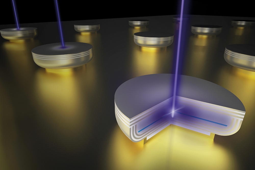
Plummeting the depths
Our partners at TU Berlin have grown our VCSEL cavity, including the quantum wells and the sacrificial layer needed for substrate removal, by MOCVD. Their starting point was an Al0.55Ga0.45N pseudosubstrate provided by FBH. The sacrificial layer that we use is actually a highly n-doped multi-layered structure, chosen partly because it enables incorporation of lower aluminium-content layers while not degrading the crystal quality of the device layers. Another merit of this particular design is that the built-in polarization fields yield sheets with high carrier concentrations. Both factors enhance etch selectivity between the sacrificial layer and the cavity, and result in a smoother etched surface.
Fabrication of the UVB VCSEL, featuring dielectric SiO2/HfO2 DBRs, has taken place in our lab (see Figure 4 for an overview of the process flow, and Figure 5 for the finished device). The VCSELs are thermo-compressively bonded to a carrier and the metal stack on top of the DBR that enables this consists of aluminium, followed by titanium and gold. The primary role of the aluminium is to strongly enhance reflectivity at the 266 nm pump wavelength. By adding this layer, we promote recycling of light that is not absorbed in the cavity on a single-pass.

Figure 5. (Left) Top-view optical microscope image of a fully fabricated
UVB VCSEL. (Right) Cross-sectional scanning electron microscopy image
of a half-VCSEL with the highly reflective DBR and AlGaN cavity. The
platinum on top is for protection of the topmost cavity layer during the
focused ion beam cut. It is not present in the full VCSEL structure.
Aside from this aluminium layer, our structure is not specially designed for optical pumping.
Instead, the architecture has been selected for future electrical injection. This means that there are no special layers for optimising the optical absorption of the pump, to ensure a high carrier concentration in the active region. There are just three thin quantum wells in the optical gain region, rather than multiple gain regions. By taking this approach, we will take a smaller step when we progress to an electrically injected device, because we will be using a VCSEL structure with an optical loss that is proven to be sufficiently low.
When evaluating our UVB VCSELs, we have considered the eight points provided in the Nature Photonics’ checklist for papers with a claim of lasing. Our view is that this list is a good starting point when considering making a claim of lasing. Researchers should regard this as a source of inspiration, while accepting that fulfilling every point might not be possible for all types of semiconductor laser. For example, to show a clear threshold for high-beta lasers since these lasers, also referred to as ‘thresholdless lasers’, have a large fraction of the spontaneously emitted photons coupled into the lasing mode and do therefore not have a clear kink in their output power versus input power curve.
As is to be expected for any VCSEL, pulsed optical pumping of our UVB design resulted in a nonlinear output intensity with pump power (see Figure 6(a)). The threshold pump power is around 10 MW cm-2.
Note that great care is required when trying to compare these threshold pump power densities with those published for blue or UVA VCSELs, or for optically pumped UV edge-emitting lasers. Complications arise from the shorter carrier lifetimes of UVB material, and difficulties in estimating the reflectivity of the pump beam from the sideband of the DBR, where reflectivity strongly varies with wavelength.
Increasing the pump power drives a shift in the output of our UVB VCSEL from a spectrally broad spontaneous emission to, above threshold, several high intensity peaks each with a narrow width – that is, less than 0.15 nm (see Figure 6(b)). Angular-resolved photoluminescence below threshold shows that there is emission in all angles and it is non-dispersive, as expected from spontaneous emission (see Figure 6 (c)). Above threshold, there is a transition to a well-defined beam with non-dispersive laser lines, a strong indication of lasing (see Figure 6(d)).
New adventures
For any emerging class of laser, the first important milestone is the demonstration of lasing under optical pumping. With this now accomplished, our next target is to make a useful VCSEL out of this optically pumped device. This goal, implying electrical operation, is far from trivial. It requires improvements in many different areas, to minimize losses and maximize modal gain, with efforts needing to include: an improvement in surface morphology, through optimisation of both the epitaxial growth and the electrochemical etch process; a reduction in defect densities; better heat removal; and the introduction of optical guiding structures. Such efforts will also reduce the filamentation that occurs in our latest devices.
Crucial to our success is the development of an electrical injection scheme. We believe that the most promising way forward is to introduce tunnel junctions, with an n-doped AlGaN-layer on top of the tunnel junction providing transverse current spreading. Recent work by other groups have highlighted the promise of the AlGaN-based tunnel junctions, but if it is to flourish in a VCSEL instead of in an LED, this junction will need to operate at a far higher current density – in the region of tens of kiloamps per square centimetre – and have a very smooth surface, to ensure low optical loss. 
Figure 6. Optically pumped UVB VCSEL characteristics. (a) Optical output
intensity at room temperature, integrated around a single lasing peak
and over the entire emission spectrum, as a function of pump power
density and energy per pulse. (b) Optical emission spectra at different
pump power densities. (c) Angle-resolved spectra in a logarithmic scale
below threshold and (d) above threshold. The green and purple circles in
(a) mark the data points corresponding to (c) and (d) and the black
dashed line in (d) marks the simulated longitudinal cavity mode. The
spectral resolution was 0.5 nm.
Time will tell whether efforts on UV VCSELs amount to just curiosity-driven research that attempts to push technology to its limits, or are a development that has a strong impact on society. Our view is that our technology will play a key role in helping to propel the VCSEL to the UVC, where it could be used to combat the spread of bacteria and viruses. We want to make these lasers as useful as their infrared-emitting cousins, providing an invisible source of light in our daily lives.
Our AlGaN-membrane technology, critical to our fabrication of the cavity, has uses beyond just UV VCSELs. We have already demonstrated that it can aid thin-film flip-chip UV LEDs. In future, it may also assist efforts to create high-quality waveguides for non-linear applications, help transfer high-power HEMTs to any desirable heat sink, realise high-quality microdisc lasers, and enable the reuse of precious GaN and AlN substrates.
In this context it is interesting to mention the German physicist, chemist and philosopher Johann Wilhelm Ritter. A pioneer of electrochemistry in the early 1800s, Ritter also proved the existence of ultraviolet light. Now, some 200 years on, it is rather fitting that we have benefitted from his research by using electrochemistry to create a UV light source. As little as he could predict that this would be one of the outcomes of his research, it is hard for us to foretell the usefulness of our AlGaN-membrane technology and short-wavelength UV VCSELs. We will leave it up to the research community to explore and demonstrate.
Further reading
- F. Hjort et al. ACS Photonics, 8, 135 (2021).
- M. A. Bergmann et al. Appl. Phys. Lett. 116 121101 (2020).
- M. A. Bergman et al. Appl. Phys. Lett. 115 182103 (2019).
- M. Kuramoto et al. Appl. Phys. Express 13 082005 (2020).
- T. Hamaguchi et al. Jpn. J. Appl. Phys. 58 SC0806 (2019).
- C. Zhang et al. ACS Photonics 2 980−986, (2015).
- M. Kneissl and Jens Rass (Editors), III-nitride ultraviolet emitters, Springer Series in Materials Science, 227 (2016).
- S. Rajan and T. Takeuchi, ch. 8 in III-Nitride Based Light Emitting Diodes and Applications, T.-Y. Seong et al. (eds.), Springer Nature Singapore Pte Ltd. (2017).
- Y.-S. Liu et al. Appl. Phys. Express 9 111002 (2016).
- Z. Zheng et al. IEEE Electronic Dev. Lett. 42 375 (2021)


