

Tackling the transparency-conductivity conundrum
Deep UV LEDs enjoy a hike in efficiency, thanks to the transparency of the MOCVD-grown tunnel junction
BY CHRISTIAN KUHN, TIM WERNICKE AND MICHAEL KNEISSL FROM TU BERLIN
There are many applications requiring a source of deep-UV emission. Radiation in this spectral domain is employed for materials processing, sensing, and disinfection targeting bacteria and viruses, including SARS-CoV-2.
Today, the incumbent source for these tasks is the mercury lamp, which is available in low-pressure or medium-pressure formats. A more promising option, though, is the LED: it is smaller, more robust, and does not require high voltages or employ toxic materials. There is also potential for production costs of this chip to fall, just like they have for its blue and white cousins.
Holding back the deep-UV LED is its low external quantum efficiency, which is limited by poor carrier injection and a low light-extraction efficiency – in short, it suffers from a transparency-conductivity dilemma. Makers of UVC LEDs tend to trade conductivity for transparency by utilising GaN:Mg p-layers for the injection of holes. While a good choice for electrical performance, GaN is compromised by its UV light-absorbing nature. Increasing the aluminium mole fraction in the p-AlGaN layers combats absorption losses, but at the expense of higher magnesium acceptor ionization energies that lead to a significant increase in the resistivities of the AlGaN:Mg layers, and in turn, the operating voltage. Another downside of AlGaN:Mg is that despite much effort, an ohmic contact is elusive. Forming such a contact is challenging, due to the large work function mismatch between UV-reflective metals and the high electron affinity of p-type III-nitrides.
A promising solution to the transparency-conductivity dilemma is to turn to a tunnel junction for hole injection. Twenty years ago, researchers incorporated this junction in visible, GaN-based LEDs for the first time (see Figure 1). This body of work showed that blue and green LEDs, as well as laser diodes, produce excellent performance when MBE provides the growth or re-growth of the tunnel junction.

Figure 1. Accelerating research efforts and rapid developments are
illustrated by the growing number of scientific publications and
citations regarding (In,Al)GaN-based tunnel junctions. This field has
been propelled by these main breakthroughs: first, the GaN-based
tunnel-junction LEDs, in 2001; and then AlGaN-based tunnel
heterojunctions and lateral activation mechanism in 2013, as well as
MOCVD-grown deep-UV LEDs in 2019.
One well-known strength of MBE is that, in contrast to MOCVD, it is well suited to realising very abrupt doping profiles that are beneficial for a tunnel-junction interface. In addition, MBE is capable of very high magnesium doping levels, such as more than 1020 cm-3, and it can avoid hydrogen passivation of magnesium acceptors and magnesium diffusion during overgrowth of the n-doped layer.
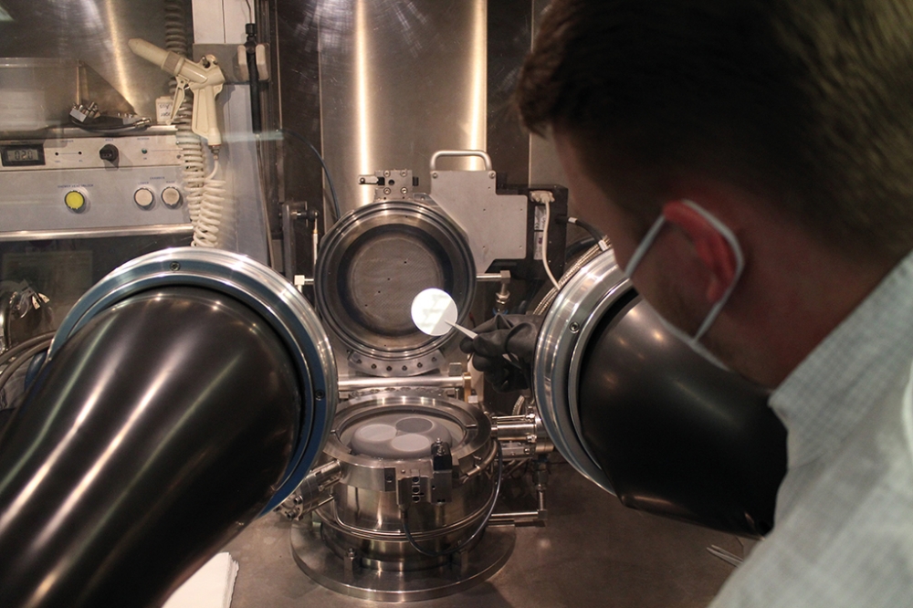
However, despite all these strengths associated with MBE, there is still much merit in trying to develop an MOCVD-based process for producing tunnel junctions. The latter is the dominant manufacturing technology for producing of III-nitride LEDs, with processes applied on an industrial scale. What’s more, the use of MOCVD allows tunnel-junction LEDs to be grown in a single run, eliminating the need for a two-step growth process.
Using this growth technology, our team at TU Berlin, Germany, has had much success developing deep-UV LEDs that incorporate a tunnel junction. We have broken new ground by demonstrating the first MOCVD-grown AlGaN-based tunnel-junctions, as well as the first AlGaN/AlGaN homojunctions; and we have produced the world’s shortest-wavelength LED that has a tunnel junction.
There are several benefits associated with the incorporation of an AlGaN-based tunnel junction in a deep-UV LED. This junction provides an alternative architecture to the conventional absorbing p-side for hole injection into the active region. With this design, which leads to hole injection via interband tunnelling, silicon-doped n-AlGaN layers partially replace highly resistive p-doped layers, and ohmic n-contacts replace rectifying p-contacts. This scheme simplifies the contact fabrication process, with the device just requiring n-metal contacts to AlGaN:Si. Further gains, stemming from the use of tunnel-junction technology for non-equilibrium hole injection, include more efficient lateral current spreading in highly conductive n-AlGaN layers and reduced optical losses in UV LEDs and laser diodes. There is also the opportunity to realise new device concepts, such as: intra-cavity contacts for VCSELs; vertical integration of cascaded laser diodes; and power adjustment by voltage-scaling, rather than current scaling. The latter refinement promises a reduction in efficiency droop.
Injection by interband tunnelling
When a tunnel-junction is incorporated into the p-side of a deep-UV LED, this leads to non-equilibrium hole injection via tunnelling (see Figures 2 and 3). Operating in forward bias, such a device produces a tunnelling of electrons from the AlGaN:Mg valence band into the AlGaN:Si conduction band. This process leaves a free hole that is injected into the active region, where it takes part in radiative recombination. The efficiency of this tunnelling may be described by a tunnelling probability.
In general, the quantum-mechanical tunnelling probability – and with that the total device resistivity – is governed by the height and the width of the tunnel barrier. The height of the barrier depends on the bandgaps of the materials at the heterojunction, while its width is determined by the space charge region. We control both characteristics with our design. Our investigation has focused on two key elements: maximizing magnesium- and silicon-doping at the tunnel junction; and the introduction of polarization-field-enhanced tunnel-junction heterostructures, which utilise lower bandgap interlayers.
We have simulated the properties of our LEDs, considering an Al0.7Ga0.3N tunnel junction (Figure 2 shows energy band diagrams at zero bias). These calculations included a reference structure with homogeneous and abrupt silicon- and magnesium-doping of 1019 cm-3 at both sides of the junction – for this structure, the space charge region is 32 nm wide. When we increase the doping levels to 1020 cm-3, the width of this region decreases to just 10 nm. Another option for reducing the width of the space charge region is to introduce polarization-field-enhanced tunnel-junction heterostructures with a GaN interlayer. This modification shortens the width of the space charge region from 32 nm down to 23 nm (see Figure 2 (b)).

Figure 2. Band diagram simulations of AlGaN-based tunnel junctions at
zero bias highlight two mechanisms for reducing the tunneling barrier
width: the heavy doping approach (a) and the heterojunction polarization
engineering approach (b). Both leads to thinner space charge regions
and higher tunneling probabilities.
Within certain limitations, there is no need to choose between these two options, but rather incorporate both of them. This has a huge pay-off, because reductions in the space charge region deliver an exponential increase in tunnelling probability, and in turn a significant hike in device performance.
We have evaluated different designs, starting with a tunnel-junction LED delivering emission in the UVC (its design is shown in Figure 3). The foundation for this device, provided by FBH Berlin, is a defect-reduced AlN-on-sapphire template formed by epitaxial lateral overgrowth of a patterned AlN layer. On this base we add, by MOCVD, aheterostructure that includes: an n type AlGaN:Si bottom current-spreading layer; a three fold AlGaN multiple quantum well, separated by AlGaN barriers; and a magnesium-doped AlGaN electron-blocking layer with a wide bandgap. For the p-side, we have a thin AlGaN:Mg short-period superlattice, followed by the tunnel junction and a top AlGaN:Si current-spreading layer. The tunnel junction features an 8 nm-thick GaN:Si interlayer sandwiched between a heavily doped AlGaN:Mg superlattice (9 x 1019 cm-3) and an AlGaN:Si layer (5 x 1019 cm-3).

Figure 3. Researchers at TU Berlin have investigated the UVC tunnel-junction LED heterostructure.
Initial emission
Fabrication of our first MOCVD-grown LEDs that feature tunnel junctions involved an in-situ thermal annealing step after the growth of the magnesium-containing layers to activate magnesium acceptors. With this step acceptor passivation by hydrogen is reduced to negligible levels – according to secondary ion mass spectrometry, the ratio of hydrogen to magnesium ions is below 10 percent. Device processing is completed with mesa etching, followed by simultaneous deposition of top and bottom V/Al/Ni/Au n-metal contacts and then a rapid thermal annealing of these contacts under nitrogen (see Figure 4 (a) for a microscopic image of our processed tunnel-junction LED, with a TU Berlin logo).
Applying a few milliamps to our device produces homogeneous emission from the whole area of the tunnel-junction LED (see Figure 4(b), which captures luminescence from the AlGaN quantum well plane using a ‘blue’ false colour). Proof of deep-UV emission comes from spectrally resolved measurements. A plot of normalized electroluminescence intensity reveals a single-peak in the UVC, centred at 268 nm, and no significant parasitic luminescence (see Figure 5 (a)). Note that these emission profiles are produced for CW injection at room temperature, for tunnel-junction LEDs with and without a GaN interlayer.
 Figure 4. Microscopic images of the processed TJ-LED surface before
operation (a) and during operation (b). In image (a), golden top and
bottom contacts are visible in bright contrast. The darker area shows
the metal-free surface of the AlGaN heterostructure, which is UV
transparent down to the multi-quantum-well plane. (b) A few milliamps
are supplied to the LED, using the top contact at the left with a black
needle attached.
Figure 4. Microscopic images of the processed TJ-LED surface before
operation (a) and during operation (b). In image (a), golden top and
bottom contacts are visible in bright contrast. The darker area shows
the metal-free surface of the AlGaN heterostructure, which is UV
transparent down to the multi-quantum-well plane. (b) A few milliamps
are supplied to the LED, using the top contact at the left with a black
needle attached.
Success on both fronts has given us two breakthroughs: the first experimental demonstration of an AlGaN-based tunnel-junction LED made by MOCVD, and the first ever AlGaN/AlGaN tunnel homojunction produced by any means.
As we expected, our variant with the homojunction has a higher tunnelling resistivity, with high voltages producing low currents. The sibling with the heterojunction produces better results. For that device, on-wafer measurements at a 60 mA drive current produce an output power up to 6.6 mW, corresponding to an external quantum efficiency of 2.3 percent and a wall-plug efficiency of 0.42 percent (plots obtained using a pulsed current are shown in Figure 5 (b)). Encouragingly, light-current and current-voltage characteristics show no indication of carrier leakage or parasitic current paths.

Figure 5. Electroluminescence spectra (a) and emission characteristics (b) of tunnel-junction LEDs emitting at 268 nm.
Using a UV-enhanced microscope camera, we have mapped the intensity across the tunnel-junction LEDs. Imaging of our finger-shaped LED mesa, with a thin central metal contact on top, shows emission from the entire mesa area (see Figure 6). The uniform emission highlights homogenous acceptor activation and current injection through the tunnel junction. If our tunnel-junction LEDs were impaired by incomplete activation or issues associated with local injection problems, this would have led to dark areas without any emission.

Figure 6. UV-sensitive microscope image of a 268 nm-emitting
tunnel-junction LED with a finger-shaped mesa geometry and central
stripe contact during operation.
Close inspection of our intensity image reveals a slight intensity enhancement near the centre compared with the finger edges. The most likely cause of this is limited current spreading in the top AlGaN:Si layer along the 170 µm long LED-fingers. This can be resolved by optimizing the LED layout or the heterostructure design through the introduction of a thicker top AlGaN:Si layer with higher conductivity.
Deeper into the UV
Our technology is capable of going deeper into the UV than the devices discussed so far, which emit at 268 nm. The fundamental limitation is the bandgap of AlN, which is just above 6 eV – this corresponds to emission at around 200 nm. Success in this domain is not easy, and gets progressively harder with every nanometre further into the deep UV. Reasons for this include: increasing severity of UV absorption; reductions in doping efficiency; limited options for carrier confinement, all issues for such LEDs in general; and lower tunnelling probabilities, resulting primarily from an increase in the tunnel barrier, due to an increase in the AlGaN bandgap and a larger space charge region.
By taking on these challenges, we have managed to expand the spectral range of our MOCVD-grown tunnel-junction LEDs down to 232 nm, a world record for this class of device (see Figure 7).
Electroluminescence spectra show a dominant emission peak from the multiple quantum wells, and only marginal parasitic long-wavelength emission from these non-optimized structures.

Figure 7. Optical and electrical characteristics and spectral power
density of a MOCVD-grown tunnel-junction LED with a peak emission at 232
nm.
Plots of current-voltage characteristics highlight one weakness of our device. Its operating voltage is above 15 V, and clearly needs to be improved. Emission power is encouraging, at almost 0.2 mW at 20 mA, helping to deliver a peak external quantum efficiency as high as 0.16 percent. For UV LEDs operating at such ultra-short emission wavelengths, this value – obtained on-wafer – is close to the highest values ever reported. In fact, it is enabled by the highly UV transparent TJ-LED heterostructure that overcomes the transparency-conductivity-dilemma of deep UV LEDs with potential for even more improvements.
The conventional approach to quantifying the efficiency of tunnelling is to use differential device resistivity (this is dV/dj, simply calculated from j-V measurements). So long as the tunnel junction provides the main contribution to device resistivity, this metric offers a solid basis for comparing different tunnel-junction LEDs.
We have compared values for device resistivity versus current density for tunnel-junction LEDs grown by MBE and MOCVD, using data reported by various groups (see Figure 8). Our plot highlights the underlying trend of decreasing resistivity with increasing current density, which occurs over several orders of magnitude and is independent of device design and growth method. One implication is that MOCVD is just as good as MBE for growing tunnel-junction LEDs.

Figure 8. Data from tunnel-junction LEDs reported by different groups
highlight the uniform trend of a decreasing differential device
resistivity (dV/dj) with increasing current density, independent of the
emission wavelength range. The growth method and the material
composition of the tunnel junction cause only small deviations from this
trend.
Another benefit of this plot, shown in Figure 8, is that it allows small variations at a fixed current density to compare properties of individual tunnel-junction LEDs. When viewed in this manner, the results highlight the outstandingly low device resistivity of nearly 10 4 Ωcm2 at 2 kAcm-2 for InGaN-based devices produced at Unipress.
Device resistivity appears to be fairly independent of the TJ’s bandgap and growth method, but it is connected to the wavelength. A low resistivity is only realised in GaN- and InGaN-based tunnel-junction LEDs emitting beyond 350 nm. When tunnel junctions employ AlGaN they show higher operating voltages as well as higher differential device resistivities due to lower achievable current densities. However, as well as the work by our team, independent efforts at Ohio State University and CRHEA-CNRS show that when tunnel junctions are formed with an aluminium mole fraction way above 50 percent – this corresponds to a bandgap above 4.5 eV – they offering an alternative approach to carrier injection that combines transparency with conductivity.
We have several ideas for improving the performance of our devices. Plans include trying to increase the wall-plug efficiency through the introduction of extra-thin AlGaN:Mg p-layers that reduce the operating voltage; suppression of donor compensation in the top AlGaN:Si layer, to improve current spreading; and a further reduction in tunnelling resistivity by optimizing doping profiles of the tunnel junction, as well as the interlayer’s composition and thickness. Once we have demonstrated high-performance tunnel-junction LEDs at the wafer level, our next step will be chip fabrication. This work will include efforts to improve yield and investigate long-term reliability, which can be easily accomplished by standard techniques used to evaluate UV LEDs.
Further reading
C. Kuhn et al. Photonics Research 7 B7 (2019)
F. Mehnke et al. Photonics Research 9 1117 (2021)
H. Amano et al. J. Phys. D: Appl. Phys. 53 503001 (2020)


