On the way to coherent VCSEL arrays

Replacing an oxide aperture with one based on the tunnel-junction
allows a shift to a planar design that facilitates the fabrication of
coherent arrays
BY ANTOINE PISSIS AND EVGENY ZIBIK FROM II-VI
DEPLOYED IN DATA CENTRES, computers, TVs and smartphones, the VCSEL is undoubtedly a great commercial success. Although it doesn’t deliver the optical power and efficiency of its edge-emitting cousin, it has the upper hand in many other regards, combining lower fabrication costs with a far, far smaller footprint and surface emission, which simplifiers testing and integration into more complex systems.
One of the key differences between the VCSEL and the edge-emitter is the approach that’s taken to confine the light and ensure optical feedback, a pre-requisite for stimulated emission. In a VCSEL, the mirrors above and below the cavity are formed from a stack of alternating layers of III-Vs that combine to create a distributed Bragg reflector (DBR). These mirrors have a very high reflectivity – it is typically around 99 percent – but they do not confine light in the lateral plane. So, to accomplish this feat in a GaAs-based VCSEL, which may emit at 850 nm or 940 nm depending on whether its has GaAs or InGaAs quantum wells at its heart, an aluminium-rich layer is added and subsequently oxidised to form an electrically insulating layer. This oxidised layer, equipped with a lower refractive index, features a non-oxidised region in the middle that acts as an aperture, confining current and guiding light. With this architecture, VCSELs are able to combine efficiency with a low threshold current, attributes that ensure commercial success.
Despite all the engineering effort devoted to its development, the oxide aperture has its limitations. One of them arises from a variation in the oxidation depth across the wafer, which makes it challenging to guarantee good reproducibility of apertures when diameters are smaller than 4 µm. A second limitation arises from having to oxidise a layer close to the active region. Due to this restriction, there is a need to etch the semiconductor through the top mirror and form a mesa around the aperture of the VCSEL, as this exposes the aluminium-rich layers to the oxidation process. A significant consequence of this pair of limitations is that it restricts the defining of an aperture of arbitrary shape, and in turn constrains the cavity geometry of the VCSEL.
Any loss of freedom when designing the cavity geometry is far from ideal. Why? Because the cavity geometry is the key design factor for selecting and promoting the resonating optical modes of the laser – and these modes govern its optical properties. Thus, if it were possible to find a way to control mode formation within the optical cavity of the VCSEL, this could extend the capabilities of this class of laser, and possibly enable it to serve new applications.
Turning to tunnel junctions
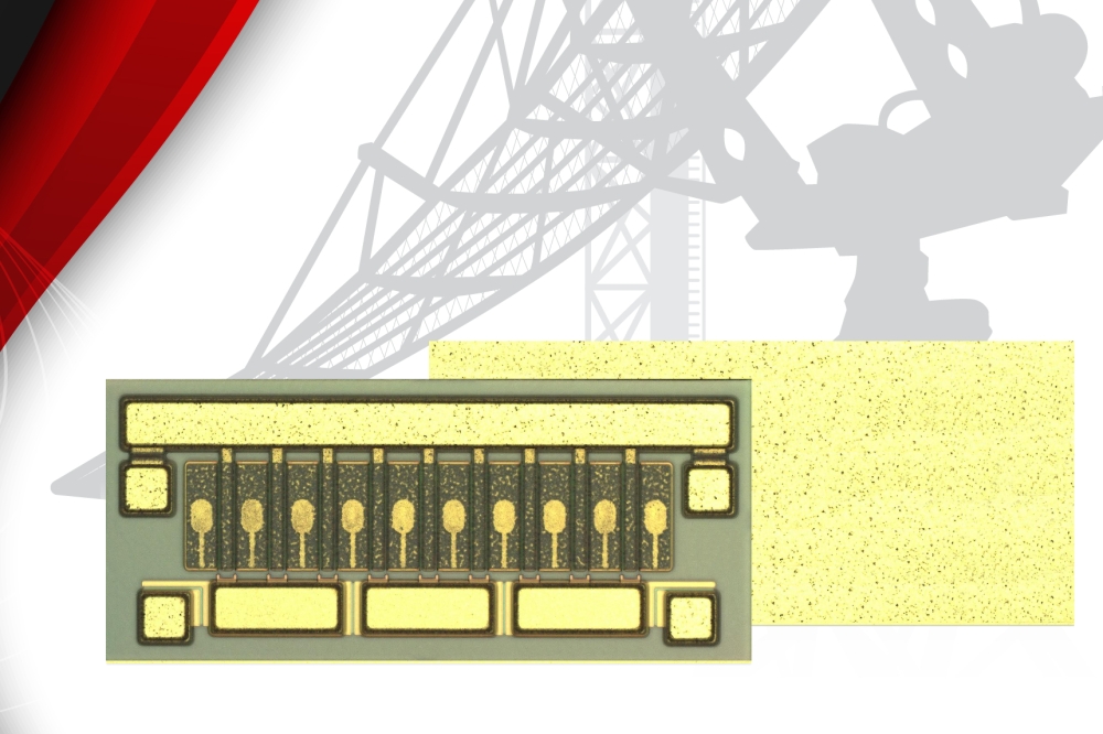
At II-VI in Zurich we have tackled the issues associated with an oxide aperture by introducing a tunnel-junction lithographic aperture. This breakthrough allows us to switch to a planar design that avoids the limitations of a mesa-based geometry. Using this architecture, we can produce VCSEL arrays, such as that with 19 elements shown in Figure 1 (due to the planar design, the 19-element array structure is not visible). Thanks to this planar design we enjoy greater flexibility, resolution, and reproducibility of all VCSEL cavities, because they are defined by lithography rather than the standard oxidation process. What’s more, our planar structure improves heat dissipation and guarantees excellent device reliability.
When manufacturers produce 940 nm VCSELs with an oxide aperture, fabrication tends to involve two steps (see Figure 2 (a)). The first is to take an n-doped GaAs substrate, load it into an MOCVD or MBE reactor, and deposit the VCSEL heterostructure that consists of an n-doped bottom DBR, a low-doped laser cavity that includes the active region, and a p-doped top DBR. After this step, the VCSEL emitter is still to be defined. To accomplish this – the second step in VCSEL fabrication – the epitaxial structure must be etched and oxidised to form the aperture of this emitter. Once this is done, the VCSEL emitter is passivated to protect it from further oxidation, and metal contacts are deposited.
We adopt a markedly different process flow when forming our tunnel-junction lithographic aperture VCSELs (an overview of this approach is provided in Figure 2 (b)). Rather than using a single growth process, we form our epitaxial structure in two sub-growth steps, separated by an aperture processing step. Fabrication begins by growing the bottom structure, consisting of an n-type bottom DBR and a partial laser cavity containing the active region. Terminating this bottom structure are highly doped p++ and n++ layers, which form a tunnel junction. Applying a direct bias to the laser leads to a reverse bias of the tunnel junction, allowing electrons and holes to tunnel through it.
With our VCSELs, optical lithography defines the area where current flows. Our etching step removes much of the tunnel-junction layers, leaving just the area that is to become the VCSEL aperture. The processed wafer that results from this localised etching is sent back to the growth reactor, where a top growth completes the epitaxial structure, adding an n-type DBR and an n-contact layer.
During the second growth, we fully define our VCSEL cavity in the vertical and lateral directions. Two of the consequences of the shallow post, formed by etching that creates a tunnel junction that is only present in the aperture area, are a local increase in the cavity optical thickness and a cavity resonance shift. This shift, equivalent to an effective refractive step, confines light laterally and restricts the VCSEL cavity in the plane of the wafer.
Another merit of our design is that by growing an n-type region over a p-type region outside the aperture, where the tunnel junction is etched away, we create an interface that acts as a p-n diode biased in the reverse direction. This provides a local blocking of current flow, thereby ensuring that current can only flow through the area containing the tunnel junction. Thanks to this design, current is laterally confined by the lithographically-defined aperture.
To complete our VCSEL fabrication process, we protect the surface with a passivation layer, prior to depositing ohmic metal contacts. Note that our process does not require any oxidation, unlike that for producing VCSELs with oxide apertures.
For VCSELs with an oxide aperture, it is the mesa lithography and the oxidation depth that define the aperture’s shape and dimension. With this process, the aperture is defined by the mesa border shape that is transferred toward the mesa centre via oxidation. With our VCSELs it is a very different state of affairs: the dimensions of the aperture are determined by the tunnel-junction’s area, which is defined by lithography. This enhances the control of the aperture shape.
We have used our approach to successfully fabricated VCSELs that have a 2 µm-diameter emitter. Our process provides good reproducibility over the entire wafer. In comparison, even with careful monitoring of the mesa oxidation depth, it is challenging to realise such reproducibility with an oxide aperture. Variations arise from local non-uniformity of the aluminium content in the oxidation layer – this influences the oxidation rate.
Our mesa-free, fully planar structure offers the possibility of fabricating dense arrays of VCSEL emitters, such as the array of 19 emitters shown in Figure 1 (in that array, VCSELs have 2 µm-diameter apertures and are arranged on a hexagonal lattice with a 5 µm pitch). One of the attributes of this array is that its footprint is smaller than that of the single mesa of an oxide aperture VCSEL emitter.
Figure 1. Optical microscopy image of a 19-emitter VCSEL array defined
by a tunnel-junction lithographic aperture. A near-field image is
presented in the inset
Measurements of this compact array reveal that it produces more than 25 mW of optical power at 25 °C, and has a power-conversion efficiency in excess of 30 percent at drive currents up to 30 mA. Near-field images show uniform current injection to all emitters within the array, thanks to the excellent conductivity of the n-doped top DBR and the tunnel junction. One consequence of such a small aperture size is that each emitter operates in single mode, resulting in a single spectral peak for the array.
Figure 2. A comparison of the fabrication process flow for a standard
oxide aperture and a tunnel-junction lithographic aperture VCSEL array.
For the same aperture size and number of emitters, the tunnel-junction
lithographic aperture process allows an arrangement that is more
compact.
Figure 3. Electro-optical characteristics in CW operation, for a
19-emitter VCSEL array defined by a tunnel-junction lithographic
aperture
Coherent control
An additional advantage of our mesa-free structure is that it opens up the possibility to exchange light between neighbouring emitters. For this to happen, the emitters need to be close enough to each other to enable evanescent coupling. When this occurs, the phase of light that’s emitted is locked, creating a coherent array, with all emitters acting as a single laser.
With our lithographic aperture technology, we can control both the emitter diameter and the spacing between emitters to an accuracy that is less than 100 nm, and is limited only by the lithography tool resolution. In comparison, in standard VCSEL arrays with oxide apertures, the presence of the mesa trenches prevents coherence, which holds the key to enhanced characteristics and high brightness.
One of the characteristics for coherent arrays is interference in the far field. We have observed this with our arrays formed from VCSELs with the tunnel-junction lithographic aperture (see Figure 4). By modifying the spacing between our emitters, we have adjusted their coupling strength. When we bring them closer together, this leads to more pronounced interference patterns. Using a 5 µm pitch between the emitters, which are 2 µm in diameter, we obtain a far-field pattern that is similar to that from a single-emitter. When we reduce this pitch to 3.3 µm or 2.5 µm phase-locking results, with the source operating as a coherent emitter array with distinct narrow far-field lobes. By controlling the optical phase shift between emitters, we alter the far-field pattern on demand. As one would expect, increasing the number of emitters increases the output power: operating at room temperature, we have realised more than 10 mW of optical power from a coherent array of 7 emitters; and in excess of 17 mW from a coherent array with 19 emitters.
Figure 4. Near-field and far-field images of a single-emitter VCSEL and a
7-emitter VCSEL array defined by a tunnel junction lithographic
aperture. The multi-lobe far-field pattern observed when decreasing the
array pitch indicates that the array is coherent.
Our tunnel-junction lithographic aperture VCSELs have an electro-optical performance that is competitive to that of their oxide-aperture counterparts. Those with a tunnel junction have a threshold current density that’s around just 2 kA cm-2; and with an optimal emitter diameter, power conversion efficiency can hit 45 percent. Such a high efficiency stems from a knee voltage of just 1.4 V, and a differential resistance of around just 100 for the epitaxial structure and 8 µm emitter diameter . This strong performance in key VCSEL characteristics demonstrates that the introduction of the tunnel junction does not induce any penalty on the performance of this class of laser.
Figure 5. Reliability performance of a 6 µm-diameter, single-emitter
tunnel-junction lithographic VCSEL stressed under 25 kA cm-2 at 125 °C.
No output optical power degradation has been observed up to 5,000 hours
of aging.
Crucially, in addition to enhanced cavity geometry control and strong performance, the tunnel junction promises excellent reliability. Our tests conducted on a 6 µm-diameter single-emitter defined by a tunnel-junction lithographic aperture uncover no sign of degradation up to 5,000 hours of aging, using a current density of 25 kA cm-2 and an operating temperature of 125 °C (see Figure 5).
We attribute this remarkable reliability to multiple factors. With our buried tunnel-junction VCSEL, the structure is stress free, thanks to the absence of lattice constant mismatch; that not the case for VCSELs with an oxide aperture, because this form of aperture introduces stress close to the active region, which can be responsible for degradation. Another advantage of our planar structure is that it improves heat removal. This reduces the thermal impedance of the device and limits its degradation, even in harsh operating conditions.
With the tunnel junction lithographic aperture, we propose an innovative technology platform, which could expand the functionality of VCSELs and open new markets and applications. Future development will continue to understand phase coupling between emitters within an array and may lead to a new class of product with beam properties that can be designed on demand.


