
Graphene-hBN breakthrough for Deep UV LEDs
Michigan study uncovers method for producing high-quality, wafer-scale, single-layer hexagonal boron nitride
In a discovery that could speed research into next-generation electronics and LED devices, a University of Michigan research team has developed the first reliable, scalable method for growing single layers of hexagonal boron nitride (BN) on graphene.
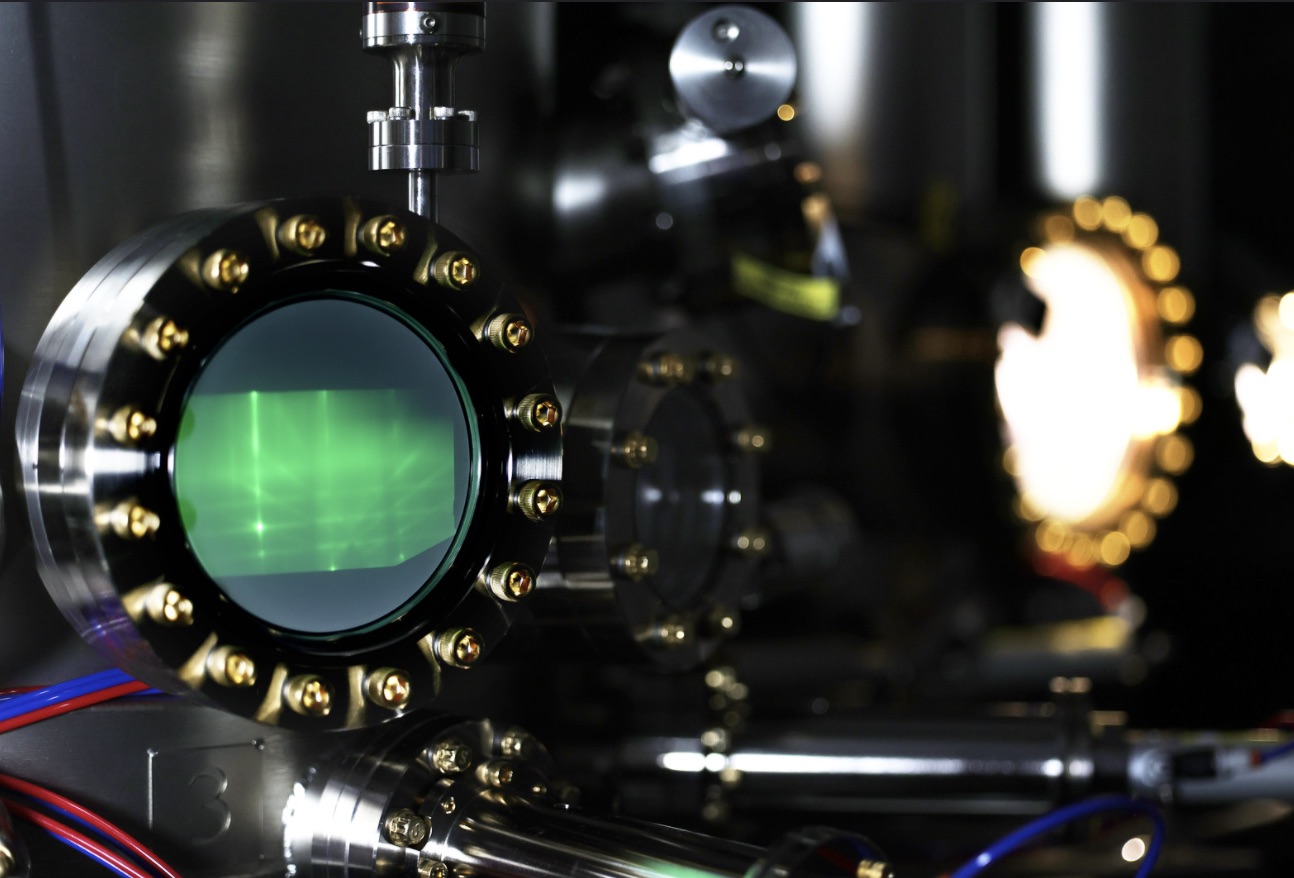
The process, which can produce large sheets of high-quality hBN with an MBE process, is detailed in the paper 'Scalable Synthesis of Monolayer Hexagonal Boron Nitride on Graphene with Giant Bandgap Renormalization' published in Advanced Materials.
Graphene-hBN structures can power LEDs that generate deep-UV light, which is impossible in today's LEDs, said Zetian Mi, U-M professor of electrical engineering and computer science and a corresponding author of the study. Deep-UV LEDs could drive smaller size and greater efficiency in a variety of devices including lasers and air purifiers.
"The technology used to generate deep-UV light today is mercury-xenon lamps, which are hot, bulky, inefficient and contain toxic materials," Mi said. "If we can generate that light with LEDs, we could see an efficiency revolution in UV devices similar to what we saw when LED light bulbs replaced incandescents."
Bonding hBN and graphene together in smooth, single-atom-thick layers unleashes a treasure trove of exotic properties. In addition to deep-UV LEDs, graphene-hBN structures could enable quantum computing devices, smaller and more efficient electronics and optoelectronics and a variety of other applications.
"Researchers have known about the properties of hBN for years, but in the past, the only way to get the thin sheets needed for research was to physically exfoliate them from a larger BN crystal, which is labour-intensive and only yields tiny flakes of the material," Mi said. "Our process can grow atomic-scale-thin sheets of essentially any size, which opens a lot of exciting new research possibilities."
While researchers have tried in the past to synthesise thin layers of hBN using methods like sputtering and CVD, they struggled to get the even, precisely ordered layers of atoms that are needed to bond correctly with the graphene layer.
"To get a useful product, you need consistent, ordered rows of hBN atoms that align with the graphene underneath, and previous efforts weren’t able to achieve that," said Ping Wang, a postdoctoral researcher in electrical engineering and computer science. "Some of the hBN went down neatly, but many areas were disordered and randomly aligned."
The team, made up of electrical engineering and computer science, materials science and engineering, and physics researchers, discovered that neat rows of hBN atoms are more stable at high temperature than the undesirable jagged formations. Armed with that knowledge, Wang began experimenting with MBE.
Wang used a terraced graphene substrate—essentially an atomic-scale staircase—and heated it to around 1600degC before spraying on individual boron and active nitrogen atoms.The result far exceeded the team's expectations, forming neatly ordered seams of hBN on the graphene's terraced edges, which expanded into wide ribbons of material.
"Experimenting with large amounts of pristine hBN was a distant dream for many years, but this discovery changes that," Mi said. "This is a big step toward the commercialisation of 2D quantum structures."
This result would not have been possible without collaboration from a variety of disciplines. The mathematical theory that underpinned some of the work involved researchers in electrical engineering and computer science and materials science and engineering, from U-M and Yale University.
Mi's lab developed the process, synthesised the material and characterized its interactions with light. Then, materials scientists and engineers at U-M and collaborators at Ohio State University studied its structural and electrical properties in detail.
Emmanouil Kioupakis, associate professor of materials science and engineering at U-M, and Jay Gupta, professor of physics at OSU, are also corresponding authors of the paper.
The research was supported by the Michigan Engineering Blue Sky Initiative, Army Research Office, National Science Foundation, U.S. Department of Energy and the W.M. Keck Foundation.


