
Steam annealing enhances the InP HEMT
Fabricated with a steam annealing step, InP HEMTs with an ultra-thin Al2O3 gate dielectric produce a high maximum-oscillation frequency over a wide bias range
Engineers from Fujitsu have realised a high-frequency performance for an InP HEMT over a wide bias range with a fabrication process that involves steam-annealing an Al2O3 gate dielectric.
This HEMT’s combination of a reduced gate leakage current, an increased forward-breakdown voltage and a maximum oscillation frequency (fMAX) that’s in excess of 700 GHz over a wide bias range, has much promise for the future of mobile communications.
When 6G is eventually rolled out, it may well use carrier frequencies in the 275 GHz to 320 GHz range to boost bandwidth compared with previous communication standards. Due to significant attenuation at these very high frequencies, amplifiers with a high output frequency will be needed, a requirement met by InP HEMTs.
Historically, this class of HEMT has been held back by a large leakage current, a low breakdown voltage and a lack of high linearity. But that’s not the case for Fujitsu’s device, which overcomes all these weaknesses with an Al2O3 gate dielectric – it is renowned for its a wide bandgap, high dielectric constant and high breakdown voltage.
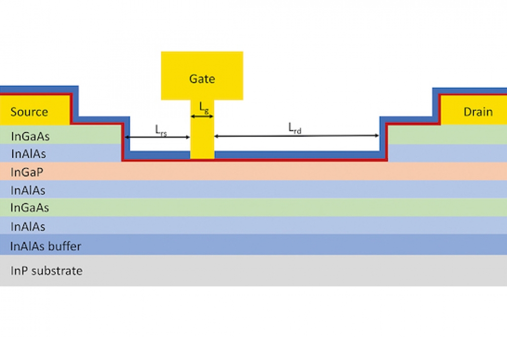
To produce this transistor, the team took an InP substrate and deposited an epitaxial stack that included a 9.5 nm-thick In0.63Ga0.37As channel and a carrier supply layer comprising a 3 nm-thick, unintentionally doped In0.52Al0.48As spacer and a 4 nm-thick, n-type In0.52Al0.48As doping layer. Selective wet etching formed a gate recess area, on which the team added a 2 nm-thick Al2O3 film, grown by atomic layer deposition. To minimise defects in this oxide, the engineers applied steam annealing for 1 hour at 300 degC.
According to work by other groups, annealing in an oxygen-containing environment enhances passivation of dangling bonds, including oxygen vacancies in oxide films. In particular, the use of steam is expected to accelerate hydrolysis of carbon impurities in Al2O3 films caused by trimethylaluminium.
Following steam annealing, the researchers added a 10 nm-thick SiN passivation layer by plasma-enhanced CVD, before defining a gate region by etching with SF6. Finally, they formed a Y-shaped Ti/Pt/Au contact (see figure above for the completed structure ). In addition, the team fabricated a control device, free from Al2O3 and featuring a Schottky gate.
To examine chemical bonds in devices before and after annealing, the team turned to Fourier transform infrared spectroscopy. Peaks associated with C-C and C-O bonds were far weaker after steam annealing, while the signal associated with the Al-O bond increased in intensity. Based on these findings, the team suggested that steam annealing enhanced the hydrolysis of carbon impurities and the passivation of dangling bonds in the Al2O3 film.
Another potential consequence of steam annealing is that it affects electron traps within the transistor. To determine whether this is the case, the team measured the sheet resistance of their HEMTs, using the transmission line method. This investigation showed that steam annealing reduced resistance in the insulated gate HEMT from 262 Ω/sq. to 211 Ω/sq. The team attributed this fall to the hydrolysis of carbon impurities and the passivation of dangling bonds.
Electrical measurements on both types of device showed that the insulated-gate HEMT had a superior transconductance profile. Thanks to this, values for fMAX and the cut-off frequency, fT, undergo very little change with gate bias. The favourable flat profile for fMAX peaks at 801 GHz, for a gate bias of 0.05 V, and is in excess of 700 GHz between -0.5 V and 0.25 V.
The team claims that its results show that its insulated-gate HEMT promises to improve the RF performance of InP HEMTs for very high frequency applications.
Picture: Fujitsu’s insulated-gate HEMT has values for gate length (Lg), LRS and LRD of 75 nm, 70 nm and 150 nm, respectively.
Reference
S.Ozaki et al. Appl. Phys. Express 15 041001 (2022)


