
Making dark semiconductors shine
International research team led by scientists at German university puts idea into practice for the first time
Whether or not a solid can emit light, for instance as an LED, depends on the energy levels of the electrons in its crystalline lattice. An international team of researchers led by University of Oldenburg physicists Hangyong Shan and Christian Schneider has succeeded in manipulating the energy-levels in an ultra-thin 2D sample of the semiconductor WSe2 in such a way that this material, which normally has a low luminescence yield, began to glow.
The team has now published an article on its research in the science journal Nature Communications.
According to the researchers, their findings constitute a first step towards controlling the properties of matter through light fields. "The idea has been discussed for years, but had not yet been convincingly implemented," said Schneider. The light effect could be used to optimize the optical properties of semiconductors and thus contribute to the development of innovative LEDs, solar cells, optical components and other applications. In particular the optical properties of organic semiconductors – plastics with semiconducting properties that are used in flexible displays and solar cells or as sensors in textiles – could be enhanced in this way.
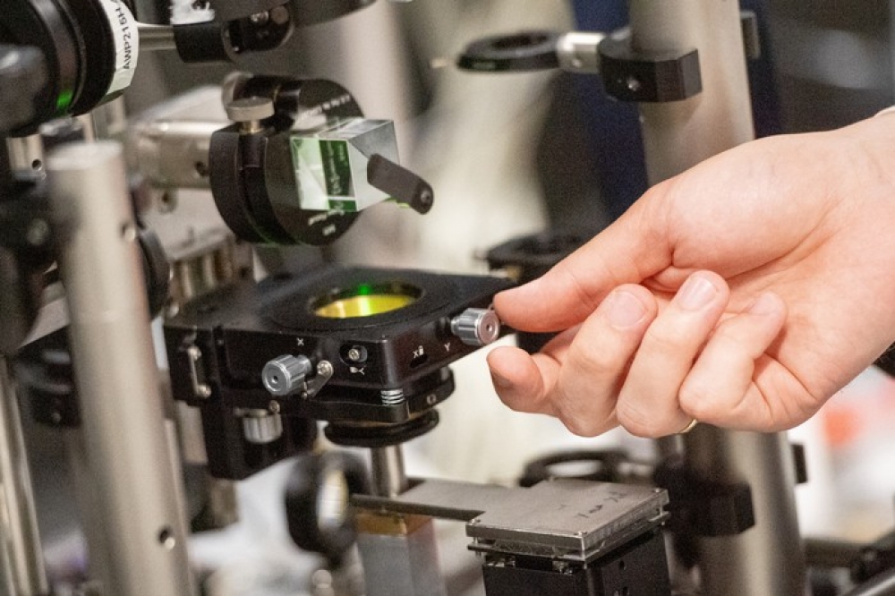
The team led by Shan and Schneider placed the 2D WSe2 sample between two specially prepared mirrors and used a laser to excite the material. With this method they were able to create a coupling between photons and excited electrons. "In our study, we demonstrate that via this coupling the structure of the electronic transitions can be rearranged such that a dark material effectively behaves like a bright one," Schneider explained. "The effect in our experiment is so strong that the lower state of WSe2 becomes optically active." The team was also able to show that the experimental results matched the predictions of a theoretical model to a high degree.
The current study is the result of a collaboration between the researchers at the Carl von Ossietzky University of Oldenburg (Germany) and colleagues from Reykjavik University (Iceland), the University of Würzburg (Germany), Friedrich Schiller University (Germany), Arizona State University (USA) and the National Institute for Materials Science in Tsukuba (Japan). Parts of the theory were developed by colleagues at ITMO University in St. Petersburg (Russia) before the universities terminated their collaboration.
Reference
'Brightening of a dark monolayer semiconductor via strong light-matter coupling in a cavity' by Hangyong Shan et al; Nature Communications volume 13 (2022)


