
ACM Introduces SiC wafer Cleaning Tool
Company builds on experience in single wet wafer cleans to enter post-CMP cleaning market
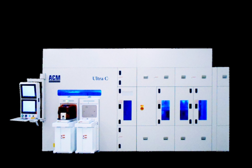
ACM Research, a supplier of wafer processing solutions, has announced its new post-CMP cleaning tool.
This is ACM’s first tool of its kind, serving as a cleaning step following the chemical mechanical planarisation (CMP) process used to manufacture high quality substrates. It is available in 6- and 8-inch configurations for SiC, and 8- and 12-inch configurations for silicon wafer manufacturing.
The tool is available in wet-in dry-out (WIDO) and dry-in dry out (DIDO) configurations, with 2-, 4- and 6-chamber options to achieve maximum throughput of up to 60 wafers per hour (WPH).
“The global equipment supply chain continues to experience extended delivery times,” said Dr. David Wang, ACM’s president and CEO. “This has created an opportunity for ACM to leverage its extensive experience in semiconductor cleaning process technology to enter the post CMP cleaning market, further expanding its cleaning portfolio. The post-CMP cleaning tool will allow ACM to help alleviate shortages facing our customers through delivery of our stable, reliable and cost-effective solution with shorter-than-average lead times.”
Following the CMP step, a physical pre-clean process is needed to reduce the number of particles, using dilute chemicals at low temperatures. ACM’s post-CMP cleaning tool is available in multiple configurations, including advanced cleaning technologies with ACM’s Smart Megasonix.
The new WIDO online pre-clean tool attaches directly to an existing CMP tool. Wafers are automatically transferred into two brush chambers, where the front-side, back-side and bevel edge are processed concurrently with chemical and cold deionized water (CDIW). Wafers are then moved to either two or four clean chambers and are processed with multiple chemicals and CDIW. A nitrogen (N2) dry and spin completes the process, which achieves a particle performance of <15 particles at or above 37nm and 20-25 particles greater than 28nm, with metallic contamination of ≦ 1E+8 (atoms/cm2) . The WIDO pre-clean tool offers a throughput of up to 35 WPH when using the four-chamber tool.
The new DIDO pre-clean tool is a stand-alone tool with four loadports and a smaller footprint than the WIDO pre-clean tool, intended for customers whose CMP platforms have a built-in cleaning chamber such that wafers come out of the tool dry. In this configuration, wafers are manually transferred to the pre-clean tool via the loadport, then processed identically to those in the WIDO pre-clean tool. The DIDO pre-clean tool is available in four- or six-chamber configurations, with two brush and two cleaning chambers or two brush and four cleaning chambers. The DIDO pre-clean tool achieves the same metallic contamination results as the WIDO pre-clean tool while delivering throughput up to 60 WPH when using the six-chamber tool.
A third available configuration is a WIDO offline pre-clean tool for use where fab floor space is at a premium. When using this tool, wet wafers are transferred from the CMP tool to a DIW bath, and then manually moved to the WIDO offline pre-clean tool, which uses the same cleaning process with the same particle performance achieved and throughput of up to 60 WPH.


