
Finwave Semiconductor Raises $12.2M
Funding is to advance 3DGaN FinFET transistors for 5G
3DGaN innovator and MIT-spin-out Finwave Semiconductor has announced a $12.2 million Series A funding round led by Fine Structure Ventures with additional participation from Citta Capital, Soitec, Safar Partners and Alumni Ventures.
The Series A follows an award of $4.3 million in federal funding from the US Department of Energy Advanced Research Projects Agency-Energy (ARPA-E) SCALEUP (Seeding Critical Advances for Leading Energy technologies with Untapped Potential) grant, to help bring the company’s technology to volume production.
The funds will be used to expand the company’s team, product development activities and lab facilities – all in advancement of Finwave’s mission to revolutionise the future of 5G communications with next-generation 3DGaN FinFET technology.
“Finwave’s technology unlocks the promise of 5G,” said Jennifer Uhrig, senior managing director at Fine Structure Ventures, a venture capital fund affiliated with FMR LLC, the parent company of Fidelity Investments. “The company combines best-in-class power amplification efficiency with high-volume manufacturing to overcome the performance and cost limitations that have together stymied widespread adoption of mmWave. We are thrilled to be working with Finwave to bring their revolutionary products to market.”
`mmWave is critical to the future of all wireless technology, but the realisation of its potential faces severe roadblocks. Weak uplink, high deployment costs, low 5G radio efficiency and soaring operating costs are all combining to thwart the promise of mmWave. Currently, 5G networks are being held back from realising their true potential due to a critical missing component: high-performance mmWave power amplifier technology.
High-performance GaN-on-Si brings a new option to the table that could make 5G millimeter wave more practical. At mmWave frequencies, GaN-on-Si amplifiers excel versus alternative solutions such as Si RFSOI MOSFETs, GaAs pHEMTs, or SiGe devices. Finwave’s award-winning 3DGaN technology significantly improves linearity, output power and efficiency in 5G mmWave systems – while greatly reducing costs for carriers. By leveraging high volume 8 inch Si CMOS fabs for producing 3DGaN chips, Finwave’s devices benefit from both the cost model and scalability of silicon technology.
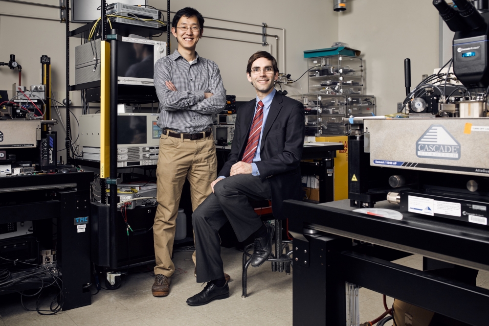
“3DGaN FinFET technology is a result of over 10 years of research and development, initially developed at MIT and recognised with the coveted 2012 IEEE Electron Device Society George Smith Award,” noted Bin Lu, Finwave’s CEO and co-founder, pictured above with co-founder Tomas Palacios. “The enormous potential of GaN FinFETs has since been demonstrated by a growing number of researchers around the world.
"Finwave was founded with the mission to scale the technology from lab to high-volume products that benefit society, and 5G presents the perfect market opportunity for the scale, performance gains and cost advantages this technology brings. Having solved numerous manufacturing challenges and successfully created a fabrication process using standard 8 inch Si CMOS tools, Finwave is leading the way in commercialising the 3DGaN technology for 5G.”
Finwave chief strategy officer and executive chairman Jim Cable added, “After spending 30 years working in the silicon on insulator technology and being an early pioneer in getting this technology into every cell phone on the planet, the opportunities for Finwave’s 3DGaN GaN-on-Silicon technology are enormous, and I am very excited to be part of the team. I personally understand the challenges of ramping up a new technology into high-volume markets, and we are very focused on all aspects of enabling this. Closing this Series A round is a major step forward for us.”


