
Scientists explore 2D semiconductors for optoelectronics
Connecting 2D perovskites to optically active transition metal dichalcogenides could improve optoelectronic device performance
New research led by scientists at Monash University in Australia looks at a methodology to improve the optoelectronic device performance and extend the functionalities of 2D perovskites by connecting them with optically active transition metal dichalcogenides (TMDs).
2D perovskites and TMDs are structurally dissimilar, however, they can form clean interfaces owing to van der Waals interactions between the stacked layers. Using accurate first principles calculations, the authors demonstrate that the novel interface (band alignment) and transport properties are feasible in 2D perovskite/TMD heterostructures which can be widely tuned based on appropriate choice of the constituents.
To understand the interface properties accurately, the authors created lattice matched structures of the interfaces and explored their properties through highly memory intensive computations using supercomputing facilities.
In specific systems, the predicted type-II alignments with NIR/visible bandgaps can enable enhanced optical absorption at comparatively lower energies. Also, sizeable band offsets and possibility of interlayer excitons with lower dissociation energies can lead to easier interlayer separation of the excited charge carriers across two materials. These render the possibility of achieving higher photocurrents and improved solar cell efficiencies. The researchers also predict the possibility of type-I systems for recombination-based devices like light-emitting diodes and type-III systems for achieving tunnelling transport. Additionally, they also show significant strain tolerance in such 2D perovskite/TMD heterostructures, a pre-requisite for flexible sensors.
“Overall, these findings demonstrate that a computationally-guided selection of heterostructures could offer better platforms than intrinsic materials for specific device applications and have potential in next-generation multifunctional devices such as flexible photosensors or LEDs”, says FLEET CI A/Prof Nikhil Medhekar who led the work with PhD student Abin Varghese and postdoctoral researcher Yuefeng Yin.
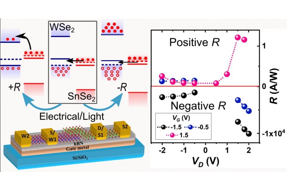
Exploring the physics of 2D heterostructures further, the team collaborated with experimentalists led by Saurabh Lodha from IIT Bombay, India to explain the emergence of a yet undiscovered optoelectronic phenomena.
In the first work on WSe2/SnSe2 heterostructures, upon illumination, the polarity of the photocurrent showed a dependence on the type of electrical transport (thermionic or tunnelling) across the interface of the heterostructure. The picture above shows how the charge transport mechanism across the WSe2/SnSe2 heterostructure can be controlled either using light or by applying an out-of-plane electric field, which can lead to positive or negative photo responsivity (R).
The researchers at Monash employed density functional theory based electric field dependent band-structure calculations and attributed this observation to the nature of band alignment at the interface. Together, they showed that a change in band alignment from type-II to type-III resulted in a change in polarity of photocurrent from positive to negative.
In terms of the performance of photodetectors, the responsivity and response time are crucial metrics. In this study a high negative responsivity and fast response time was experimentally observed in the device prototypes which are encouraging for further development of 2D materials-based devices for practical applications.
In another heterostructure comprising black phosphorous and MoS2, the experiments illustrated an illumination wavelength-dependence on the polarity of photoconduction. The negative photoconductance seen at specific wavelengths above the absorption edge of MoS2 could be controllably and reversibly tuned to positive photoconductance at lower wavelengths. The threshold wavelength for crossover between negative and positive photoconductance had a crucial dependence on the flake thicknesses. Thickness-dependent band-structure calculations carried by researchers from Monash clearly showed the possibility of an increase in recombination of charge carriers for specific thicknesses which could lead to negative photoconductance, thus aiding the conclusions.
These studies demonstrate new methods to control the sensing mechanism in photodetectors which has not yet been studied in such details.
References
'Near‐Infrared and Visible‐Range Optoelectronics in 2D Hybrid Perovskite/Transition Metal Dichalcogenide Heterostructures'; Advanced Materials Interfaces (2022)
'Polarity-Tunable Photocurrent through Band Alignment Engineering in a High-Speed WSe2/SnSe2 Diode with Large Negative Responsivity' ; ACS Nano (2022)
'Wavelength-Controlled Photocurrent Polarity Switching in BP-MoS Heterostructure'; Advanced Functional Materials (2022)


