
Laser lift-off yields superior flexible HEMTs
Flexible transistors with minimal degradation are produced with a lift-off process that involves a UV laser and GaN-on-sapphire HEMTs
Many different approaches can produce flexible GaN HEMTs via transfer technologies. But all lead to more damage to this device than laser lift-off, according to engineers from the University of South Carolina.
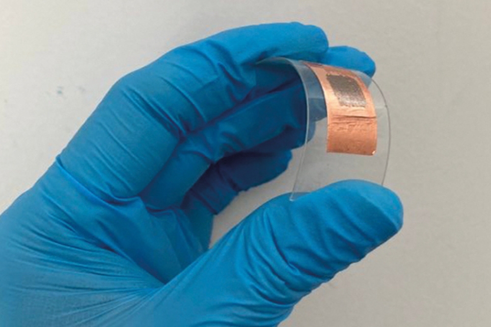
Using a 193 nm excimer laser, researchers at that university have recently transferred GaN-on-sapphire HEMTs to a copper tape that is mounted on a flexible, transparent plastic. It is a process that leads to a decline in the drain current of the HEMT by just 18 percent – that’s far less than the fall in that figure-of-merit resulting from a range of other transfer techniques, all based on etching GaN-on-silicon HEMTs.
Flexible GaN HEMTs are attracting a great deal of attention because they can serve in many applications. Illustrating this point, team spokesman Md Didarul Alam remarks: “The device has great potential in applications for on-screen power amplifiers in mobile phones, strain-controlled power devices in bio-inspired electronics, such as acceleration-feedback-control in self-driving cars or robotic motion, and human-machine interfaces.” There are also opportunities for flexible GaN HEMTs in high-frequency microwave power applications, such as reconfigurable antenna; and in high-power conformal and flexible RF devices that are compatible with 5G communication systems.
Most efforts at developing processes for transferring GaN HEMTs to a flexible substrate have focused on mechanical grinding of the GaN-on-silicon epiwafer, followed by XeF2 etching and wet etching. One weaknesses of this approach is a degraded backside, caused by a harsh acidic environment, as well as the strong surface tension of water.
An alternative is to grow uniform large-area hexagonal BN between the AlGaN/GaN heterostructure and substrate, prior to peeling off the nitride membrane. But mechanical transfer is difficult, argues Alam, saying that it is hard to completely peel off a large-area AlGaN/GaN membrane.
There’s also electrochemical etching, which involves a highly doped GaN sacrificial layer. However, this layer damages the effective area and compromises the integrity of the released GaN heterostructure.
As well as these issues, which lead to a far greater decline in the drain current after transfer to a flexible foundation, there is another drawback: the production of the epiwafers, all based on GaN-on-silicon, is complicated and time-consuming. Part of the problem is that the epitaxial growth of GaN-on-silicon demands additional growth steps, due to the significant mismatches in both the lattice constant and the coefficient of thermal expansion between the two materials families. In addition, the quality of the GaN epilayer is inferior to that formed on sapphire, SiC or bulk GaN.
Alam and co-workers produced their flexible HEMTs by depositing on a double-side polished sapphire substrate a 30 nm-thick GaN nucleation layer, a 1.8 mm-thick GaN buffer and channel layer, a 1 nm-thick AlN spacer, and a 17 nm-thick Al0.24Ga0.76N barrier layer. Reactive-ion etching created mesas from the epiwafer, before electron-beam deposition and subsequent rapid thermal annealing formed source and drain electrodes, and electron-beam evaporation added a gate electrode. Devices were temporarily bonded to UV tape before an ArF 193 nm laser delivered a fluence of 800 mJ cm-2 to remove the sapphire. Etching with dilute HCl eradicated the damage to the GaN layer, prior to bonding to the flexible substrate.
Measurements showed that this HEMT’s maximum drain current fell from 422 mA mm-1 to 347 mA mm-1.
One of the next goals for the team is to fabricate flexible HEMTs with an AlGaN-channel. “Since the critical electric field of AlGaN is higher than that of the GaN, AlGaN-channel flexible HEMTs will be more suitable for high-frequency and high-power flexible electronics applications,” says Alam.
Reference
M.D. Alam et al. Appl. Phys. Express 15 071011 (2022)


