
MoS2 could help shrink lasers
Microscopic colour converters move small laser-based devices closer to reality
Working in James Schuck’s engineering lab at Columbia, PhD student Xinyi Xu and postdoc Chiara Trovatello from Politecnico di Milano in Italy, have been studying how efficiently devices built from stacks of 2D MoS2 can convert light frequencies at telecom wavelengths to produce different colours.
They believe this new research could be a first step toward replacing the standard materials used in today’s tuneable lasers.
2D MoS2is one of the most studied transition metal dichalcogenides. Single layers of MoS2 can convert light frequencies efficiently, but are actually too thin to be used to build devices. Larger crystals of MoS2 meanwhile, tend to be more stable in a non-colour converting form. To fabricate the necessary crystals, known as 3R-MoS2, the team worked with the commercial 2D-material supplier HQ Graphene.
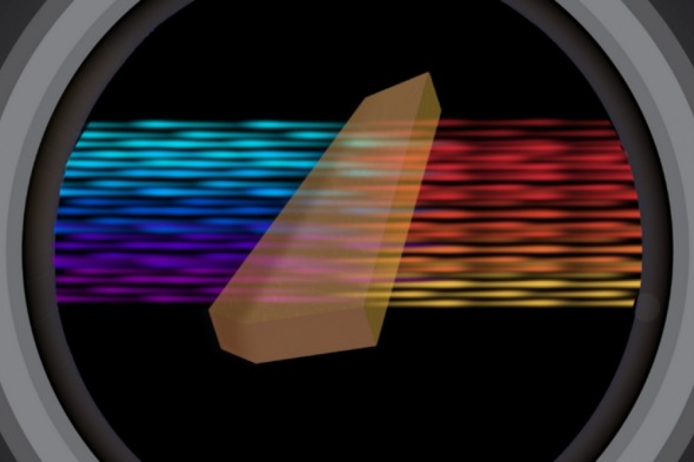
With 3R-MoS2 in hand, Xu began peeling off samples of varying thickness to test how efficiently they converted the frequency of light. Right away, the results were spectacular. “Rarely in science do you start on a project that ends up working better than you expect—usually it’s the opposite. This was a rare, magical case,” remarked Schuck. Usually, special sensors are needed to register the light produced by a sample, and it takes some time for them to do so, explained Xu. “With 3R-MoS2, we could see the extremely large enhancement almost immediately,” he said. Notably, the team recorded these conversions at telecom wavelengths, a key feature for potential optical communications applications, such as delivering internet and television services.
In a fortunate accident during one scan, Xu focused on a random edge of a crystal and saw fringes that suggested waveguide modes were present inside the material. The team handed their devices off to the lab of physicist Dmitri Basov, where his postdoc Fabian Mooshammer confirmed their hunch.
Currently, the most popular crystal for waveguided conversion and generating entangled photons is lithium niobate, a hard and stiff material that needs to be fairly thick for achieving useful conversion efficiencies. 3R-MoS2is equally efficient but 100 times smaller and flexible enough that it can be combined with silicon photonic platforms to create optical circuits on chips, following the trajectory of ever-smaller electronics.
With this proof-of-concept result, the bottleneck toward real-life applications is large-scale production of 3R-MoS2 and high-throughput structuring of devices. There, the team says, industry will need to take over. With this work, they hope they’ve demonstrated the promise of 2D materials.
“I’ve been working on nonlinear optics for more than thirty years now. Research is most often incremental, slowly building on what came before. It’s rare that you do something completely new with big potential,” said Giulio Cerullo, a nonlinear an optics researcher at Politecnico di Milano in Italy. “I have a feeling that this new material could change the game."
Work at Columbia was supported by the US Department of Energy-funded Programmable Quantum Materials Energy Frontiers Research Centre. Work at Politecnico di Milano was supported by the European Union’s Horizon 2020 Research and Innovation Program.
'Towards compact phase-matched and waveguide nonlinear optics in atomically layered semiconductors' by Xinyi Xu, Chiara Trovatello, et al; Nature Photonics (2022)


