
Bringing down the cost of III-V epitaxy
A radical form of HVPE that speeds growth, ensures high-quality
interfaces, and allows the inclusion of aluminium-containing alloys will
revolutionise production of III-V devices.
BY AARON PTAK, JOHN SIMON AND KEVIN SCHULTE FROM NREL
III-V semiconductors are the gold standard for many devices. They sit at the heart of lasers and LEDs, high-speed and high-power electronics, and space photovoltaics (PVs). Consider, for example, the latter: PVs made from III-Vs have demonstrated the highest energy-conversion efficiency and specific power for any material system, and can be very lightweight, thin and flexible, as well as incredibly stable – that’s everything anyone would want from a solar cell. What III-Vs are not, however, is cheap – at least on a cost-per-area basis – due to a lack of driving force to make them so.
For many devices, including transistors, cost-per-area is not a major issue. That’s because the high cost is amortized through the production of thousands and thousands of devices from every wafer. However, some applications don’t have this luxury, including PV – both solar and thermal – and microLEDs deployed to populate substantial display areas.
Again, using solar cells as an example, it costs between $30,000 and $50,000 to cover a square meter with high-efficiency III-V PV, while the equivalent cost for silicon solar cells is at least two orders of magnitude lower. Due to this significant disparity, the III-V team at the National Renewable Energy Laboratory devoted much effort in developing concentrating photovoltaics (CPV), motivated by the hope that the high cost of solar cells would be offset by relatively cheap aluminium, glass, and steel. Unfortunately, due largely to plummeting prices of silicon PV over the last decade, the CPV market never materialized.
Our new challenge is to make III-V devices competitive in one-Sun, non-concentrated applications where the benefits of thin, light, flexible, stable, high-efficiency III-V PV can truly shine. These attributes will allow III-Vs to be deployed in applications where today’s more prevalent solar technologies cannot, such as powering unmanned aerial vehicles, or being moulded into car bodies and integrated into architecture in ways that are more aesthetically pleasing. But there is a problem of scale. As each 6-inch III-V wafer produces just 4-5 W of power, the area required to produce megawatts, let alone the gigawatts needed to power an increasingly electrified world, is astonishing.
If these III-V devices are to move from niche markets, such as space PV, to widespread terrestrial applications without the aid of concentration, their cost will have to tumble. Success on this front would be welcome throughout the compound semiconductor community. Even for producers of devices where the size of the chip is a secondary matter, due to demand for III-Vs rising across the board, a substantial fall in cost would be good news.
Cost drivers
Three main factors contribute to the cost of producing III-V devices: the price of the substrate, the expense associated with the epitaxial process, and device processing. Substrate production costs have fallen in recent years, driven by increased demand for VCSELs and other optoelectronics, while post-processing has benefitted from higher levels of automation. The cost of epitaxy, however, has remained stubbornly high, which is why we have been focusing on an approach to slash the cost of epitaxial growth. Today’s MBE and MOCVD tools are batch systems, which limit throughput and hamper scaling to very large production volumes. Growth involves either relatively expensive precursors, used inefficiently, or costly high-vacuum equipment. What’s needed, especially for area-intensive device applications, is a low-cost, high-throughput and easily scalable deposition method that produces materials and devices with the same quality as the incumbent approaches.
We see HVPE as an exciting possible solution. Developed between the 1960s and the 1980s, this growth technique is well known for using high growth rates to produce high-quality III-Vs with excellent purity from inexpensive source materials (see Figure 1).

Figure 1. Conventional HVPE growth process.
In its heyday, engineers produced a number of devices by HVPE, including commodity GaAsP visible LEDs, grown on compositionally graded buffer layers on GaAs substrates. HVPE was well-suited to producing this type of device. High growth rates could accommodate relatively thick graded layers that minimize the dislocation density, but were to blame for an incapability to produce high-quality p-n junctions – this weakness stemmed from the challenges in realising abrupt changes in the growth chemistry within the HVPE reactor. To sidestep these challenges, p-n junctions were created by diffusion. This workaround offers an insight into why HVPE has not been applied to complex device structures.
Limitations of traditional HVPE
Refinements to MBE and MOCVD growth technologies throughout the 1980s enabled these techniques to outperform HVPE, which gradually fell out of favour. The two alternatives that now dominate III-V epi-growth have three major advantages over traditional HVPE: wide, easily controlled process windows; the ability to create structurally- and chemically- abrupt interfaces between device layers; and a wider palette of materials, including aluminium-containing alloys like AlGaAs and AlGaInP that were notoriously difficult to grow by HVPE.
Here we discuss the challenges of traditional HVPE in more detail, before outlining our solutions thatare making HVPE relevant in today’s epitaxy landscape.
With traditional HVPE, the growth rate is governed by the reduction of As-Ga-Cl species on the surface by active hydrogen. The energy barrier to crack molecular hydrogen limits growth rates at lower growth temperatures, while decomposition is an important factor at higher temperatures. These trends are behind an ‘inverted U-shaped’ growth rate dependence on temperature (see Figure 2). In comparison, growth rates for MBE and MOCVD are temperature insensitive over a large temperature range. In short, while HVPE boasts higher growth rates, it fails to provide a wide, temperature-independent process window that simplifies the growth of a targeted layer thickness or alloy composition.

Figure 2. Growth rate of GaAs grown by HVPE using different metal
chloride partial pressures. The growth rate is limited by kinetics at
low temperature and the effects of decomposition at higher temperature.
The HVPE process involves in situ generation of metal chlorides – realised through the reaction of metallic gallium and indium with anhydrous HCl – that provide group III precursor species. This reaction typically takes place in a hot quartz ampoule within the reactor. When growing a layered stack of different materials, there’s a need to stop the reaction, purge out the products and change to a new chemistry – but this takes up valuable time. Speeding this up is not easy, as there is significant chemical inertia in the process, and attempts to do so can lead to graded interfaces (see Figure 3). The high growth rates inherent in HVPE exacerbate the extent of the graded material. Due to this challenge, the traditional HVPE process is incapable of growing the abrupt heterointerfaces required for today’s modern, complex device structures.

Figure 3. Schematic representation of heterostructure growth using traditional- and Dynamic HVPE.
Two of the critical materials for realizing many high-efficiency device structures, from lasers and LEDs to transistors and solar cells, are AlGaAs and AlGaInP. Roles undertaken by these high-bandgap materials include providing the cladding layers for other materials, and acting as an active layer in devices operating in the visible domain. In HVPE, the analogous aluminium-containing precursor to the standard Ga and In precursors, GaCl and InCl, is AlCl. However, this molecule is extremely reactive. It etches quartz, the most common HVPE reactor material, and is likely to pyrolyze and deposit on reactor walls before it even reaches the substrate unless the reactor runs at 1000°C or more. These temperatures are incompatible with the incorporation of relatively volatile indium-containing molecules, and so preclude the formation of AlInP and its related alloys. Even when AlCl reaches the substrate, it has such a fast reaction with the group V source that it outcompetes all other precursors, leading to the formation of AlAs instead of controllable ternary and quaternary alloys.
HVPE reimagined – Dynamic HVPE
Driven by the need to drastically reduce the cost of IIIV PV for all applications, we have spent the last decade revisiting, refining, and reinvigorating HVPE to exploit its beneficial properties while minimizing the negatives. Our key innovation is to keep the process gases constant and move the wafer, rather than keeping the wafer stationary while changing the reactant gases, as is the case in traditional epitaxy (see Figure 3). This single change completely sidesteps traditional HVPE’s chemical inertia, which is behind the graded interfaces.
We have named our approach Dynamic HVPE, to differentiate this process from traditional HVPE. With the conventional form of HVPE, changing process gases to transfer from the deposition of one material to another leads to significant growth time under a mixed atmosphere containing both gases. That’s undesirable, tending to result in substantial growth of graded-composition material, due to growth rates that are often in excess of 1 mm/min.
To address this issue, Dynamic HVPE employs two adjacent growth chambers, each prepared with steady-state gas flows and growth conditions, and a wafer that moves between them in less than two seconds, leading to chemically- and structurally-abrupt heterointerfaces. According to energy dispersive X-ray spectroscopy measurements taken in a transmission electron microscope, undertaken on a GaAs/GaInP heterointerface, Dynamic HVPE ensures atomic-scale interface abruptness (see Figure 4).

Figure 4.Energy dispersive X-ray spectroscopy measurements showing a
chemically-abrupt GaInP/GaAs heterointerface deposited by Dynamic HVPE.
Such a high degree of interfacial control holds the key to significant improvement in device performance compared with devices grown by traditional HVPE using growth pauses. For double heterostructures, a common feature in many optoelectronic devices, our superior form of HVPE provides a five-fold decrease in the interface recombination velocity, according to time-resolved photoluminescence. This indicates that Dynamic HVPE is suitable for the production of arbitrarily complex device structures that rely on low-defect interfaces for high-performance operation.
Precisely controlling rapid growth
Building on this success, we moved next to tackle the challenge of process controllability. Due to the temperature dependence of the growth process, caused by the large activation energy of the chlorine reduction step, minor changes in temperature can produce drastic variations in growth rates and alloy compositions. In traditional HVPE, the hydrogen atoms that are responsible for reducing chlorine on the surface and opening new surface sites for arsenic adsorption typically come from the hydrogen ambient used for growth. As molecular hydrogen pyrolysis kinetics are quite slow at typical growth temperatures – that is, there is limited cracking – the chlorine reduction process is very inefficient.
Cracked hydride gases, such as arsine, offer another potential source of active hydrogen species. However, arsine cracks almost immediately under typical hot-wall HVPE growth conditions, so relatively little active hydrogen would reach the growing surface.

Figure 5. Comparison of the GaAs growth rate temperature dependence for
traditional (curves) and hydride-enhanced HVPE (red points).
Hydride-enhanced HVPE maintains high growth rates at much lower
deposition temperatures.
Our solution to combatting the chlorine reduction rate-limiting step is to provide more active hydrogen where it’s needed – at the surface. We accomplish this by introducing uncracked hydride gases to the surface, where they quickly break apart. This populates the surface with a large amount of active hydrogen, which scavenges chlorine from gallium and open sites to arsenic adsorption. This fundamental change transforms HVPE from a kinetically-limited growth process that needs high temperatures to realise high growth rates, to a mass-transport-limited process that is insensitive to growth temperature. Armed with this attractive modus operandi, HVPE is aligned with incumbent growth techniques.
With Dynamic HVPE, growth rates are tremendously fast – so much so that we can measure them in millimetres per hour, rather than the microns per hour. For GaAs, we have demonstrated rates in excess of 0.5 mm/h (see Figure 5). Critically, these extreme growth rates still lead to excellent device performance, a point illustrated in measurements of the open-circuit voltage of a solar cell (see Figure 6).
We observe very little change in performance for growth rates from just less than 50 mm/h to 300 mm/h – and the change that is apparent is fully accounted for by decreasing doping levels with higher growth rates at constant doping flow.

Figure 6. Performance of GaAs solar cells grown at a high rate using the hydride-enhanced mechanism.
Solving the aluminum issue
Growing aluminium-containing materials is challenging. Our solution is to switch the precursor from the highly-reactive AlCl to the more stable AlCl3. To produce AlCl3 from Al and HCl, while avoiding having significant formation of AlCl at the same time, we employ lower temperatures than those normally present in a HVPE system. For the growth of aluminium-containing alloys we use temperatures near 400 °C, realised by either introducing a colder region inside the reactor or adding an external AlCl3 generator – each solution brings its own benefits and challenges.

Figure 7. Single- and dual-junction III-V solar cells incorporating AlInP window layers.
Using AlCl3 enables the controllable formation of AlGaAs alloys across the entire composition range, as well as the growth of Al(Ga)InP, which was long deemed impossible by HVPE. The epilayers produced by this approach still contain oxygen and silicon impurities, presumably from either wall reactions with the small amount of monochloride formed along with the trichloride, or from monochloride formed on the substrate surface. However, this work is in its infancy, and there is ample room for optimization.
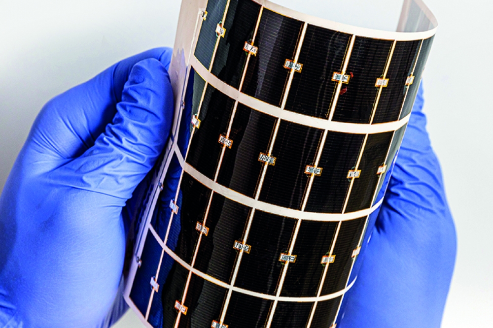
Despite these challenges, we have been able to incorporate aluminium-containing materials into devices, including single- and dual-junction solar cells that incorporate AlInP window layers (see Figure 8). The efficiency of these cells is increasing, closing the gap with MOCVD-grown devices.

Figure 8. Transmission electron microscopy and energy dispersive
electron diffraction measurements of a portion of a GaInP/GaAs DBR
structure grown using Dynamic HVPE (top), and the measured reflectance
of the DBR (bottom).
By solving the three limitations of HVPE – the lack of sharp interfaces, variations in growth conditions with temperature, and the challenge of growing aluminium-containing alloys – we have broken down the barriers to matching the performance of devices grown by today’s mainstream technologies. Now there’s the opportunity to combine the quality associated with MBE and MOCVD with lower costs and a far higher throughput.
To showcase the capability of Dynamic HVPE for the growth of a wide variety of devices we have fabricated three types of non-solar structure: a distributed Bragg reflector with 20 pairs of GaInP/GaAs that provides high reflectance at a wavelength of around 900 nm, confirming thickness control and flat, parallel interfaces (see Figure 8); a one-off growth of a HBT (not shown) that displays current modulation and gain, indicating initial proof-of-concept for transistor growth by Dynamic HVPE; and a compositionally-graded GaInP buffer layer, grown on a GaAs substrate to a lattice mismatch of 3.8 percent (not shown), that has the same dislocation density as MOCVD-grown structures. This buffer takes less than 10 minutes to grow. These results with all three structures underscore the promise of Dynamic HVPE, a technique that combines very fast growth rates with inexpensive precursors and a tremendous potential for achieving enormous scale for a vast range of devices, including VCSELs, LEDs, thermophotovoltaics and emitters/receivers for power beaming.
The path ahead
Scale is the most potent cost-reduction tool available for semiconductor growth, crucially for large-area devices. Increasing throughput delivers cost savings throughout production. Even devices with a relatively small footprint benefit from trimming cost and the ability to easily expand production when needed. By turning to Dynamic HVPE, chipmakers can employ an approach that opens the door to much greater scale for the production of III-V devices.

Figure 9. Schematic representations of the pilot-production Dynamic HVPE
reactor scheduled for delivery to NREL in Fall 2022 (top), and a
concept of the fully-inline production reactor capable of producing
500,000 wafers per year.
The dynamic wafer transfer process, which we have validated in our research reactor, is inherently scalable, so it lends itself perfectly to a fully in-line production system. In Figure 9 we offer an illustration of an in-line Dynamic HVPE system capable of producing multi-junction III-V solar cells. Note that the number and capability of the different chambers could be adjusted for any arbitrary device structure with any number or type of layers. We estimate that a system such as this could produce 500,000 wafers per year – that’s approximately 70 times that of today’s batch systems. This leap in throughput will slash costs, in addition to meeting future production demands.
As a first step toward this high-throughput production future, we are soon to take delivery of a pilot-scale Dynamic HVPE system featuring three growth chambers, to simulate a pseudo in-line growth reactor. This system will shuffle 6-inch wafers back and forth to build up a full device structure, rather than wafers moving continuously in one direction. Even the production volume of this pilot system should reach 80,000 wafers per year, equating to 300 kW of one-Sun, non-concentrated PV.
We are planning to commission our new system this Fall, before optimising its performance for device quality and throughput of high-efficiency multi-junction III-V PVs. Success on these fronts will represent a major step towards drastically lowering the cost of III-V solar cells and providing a pathway to lower cost and larger scale for all III-V devices.
Visit NREL.gov to learn more about lower-cost III-Vs and licensing opportunities.
Approved for public release; distribution is unlimited. Public Affairs release approval # AFRL-2022-4382. The views expressed are those of the author and do not necessarily reflect the official policy or position of the Department of the Air Force, the Department of Defense, or the U.S. government.
Further D.W. Shaw “Epitaxial GaAs Kinetic Studies: {001}Orientation”, J. Electrochem. Soc. 117 683 (1970)
† K.A.W. Horowitz et al. “A Techno-Economic Analysis and Cost Reduction Roadmap for III-V Solar Cells”, NREL Technical Report NREL/TP-6A20-72103 (2018) [https:// www.osti.gov/biblio/1484349-techno-economic-analysis- cost-reduction-roadmap-iii-solar-cells]
† J. Simon et al. “III-V-Based Optoelectronics with Low-Cost Dynamic Hydride Vapor Phase Epitaxy”, Crystals 9 3 (2019) [https://www.osti.gov/biblio/1488632-iii-based optoelectronics-low-cost-dynamic-hydride-vapor-phase-epitaxy]
† K.L. Schulte et al. Inverted metamorphic GaInAs solar cell grown by dynamic hydride vapor phase epitaxy Appl. Phys. Lett. 119 092101 (2021) [https://www.osti.gov/biblio/1821416-inverted-metamorphic-gainas-solar-cell-grown-dynamic-hydride-vapor-phase-epitaxy]
† W. Metaferia et al. “GaAs Solar Cells Grown at Rates >300 µm/h by Atmospheric-Pressure Dynamic HydrideVapor Phase Epitaxy”, Nat. Commun. 10 3361 (2019) [https://www.osti.gov/biblio/1619643-gallium-arsenide-
solar-cells-grown-rates-exceeding-hydride-vapor-phase-epitaxy]
† E.M. McClure et al. “GaAs Growth Rates of 528 µm/h Using Dynamic-Hydride Vapor Phase Epitaxy with a Nitrogen Carrier Gas”, Appl. Phys. Lett. 116 182102 (2020) [https://www.osti.gov/biblio/1659831-gaas-growth- rates-using-dynamic-hydride-vapor-phase-epitaxy- nitrogen-carrier-gas]
† K.L. Schulte et al. “Growth of AlGaAs, AlInP, and AlGaInP by Hydride Vapor Phase Epitaxy” ACS Appl. Energy Mater. 2 8405 (2019) [https://www.osti.gov biblio/1580495-growth-algaas-alinp-algainp-hydride-vapor
phase-epitaxy] OSTI links provided for free access)


