
Ayar Labs partners with DoD on optical I/O
Project KANAGAWA aims to transition optical I/O into the defence industrial base
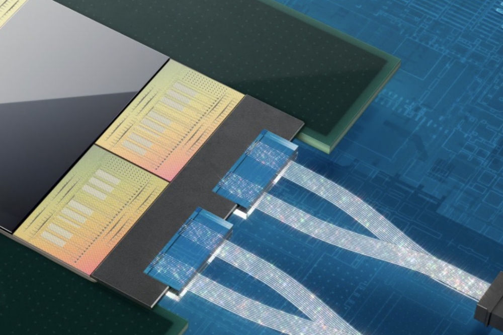
Optical I/O company Ayar Labs was awarded a $15 million multi-year prototype Other Transaction Agreement (OTA) in support of Project KANAGAWA (the Co-Packaged Analog-Drive High-Bandwidth Optical Input/Output Project).
The OTA, a non-traditional government contracting method for fast tracking research and innovation, was issued by Naval Surface Warfare Center (NSWC), Crane Division to support the Office of the Under Secretary of Defense, Research & Engineering (OUSD(R&E)) Trusted & Assured Microelectronics (T&AM) program.
This project will promote the next-level development of Ayar Labs’ optical interconnects to lead its transition into the DoD’s advanced packaging ecosystem.
“We look forward to working closely with Ayar Labs as part of Project KANAGAWA to benchmark its optical I/O chiplets and lasers toward the transition of this technology into large-scale defense applications,” said Joshua Hawke,cChief engineer of RF & Optoelectronics, NSWC Crane, Radar Technologies Division and Execution Lead of the OUSD(R&E) Trusted & Assured Microelectronics program.
During the first phase of Project KANAGAWA (Task A), Ayar Labs will deliver its optical I/O chiplets and lasers at data rate bandwidth levels exceeding 2 Tbps and energy losses below 5pJ/bit. In phase two of the project, running parallel to Task A, Ayar Labs will collaborate with Intel, Lockheed Martin and Qorvo to develop and demonstrate co-packaged optical I/O solutions built on TeraPHY optical I/O chiplets and SuperNova multi-wavelength lasers, with the goal of advancing the supply chain ecosystem for domestic manufacturing of Ayar Labs’ optical I/O solution.
“Project KANAGAWA comes at an important time for both our nation and Ayar Labs as we look to mature U.-based manufacturing for our optical I/O solutions,” said Charles Wuischpard, CEO of Ayar Labs. “We are excited to partner with the DoD, Intel, Lockheed Martin and Qorvo to not only strengthen our nation’s security by establishing domestic production of our optical I/O chiplets but also introduce next-generation defence architectures and systems.”
Co-packaged optics, which brings together photonic integrated circuits with electronic integrated circuits inside multi-chip packages (MCP), extends the reach of high-bandwidth data I/O. MCPs based on Ayar Labs’ optical I/O can generate dramatically higher data rates from the field-programmable gate arrays (FPGA) that process digital beamforming signals, opening the door to new phased array radar architectures, according to the company.
Ayar Labs expands executive team and space
Ayar Labs has expanded its executive team to further commercial development, with the addition of Lakshmikant (LK) Bhupathi, VP of products, strategy and ecosystem, and Scott Clark, VP of manufacturing and operations.
In these newly created roles, Bhupathi and Clark will focus on product management, manufacturing, supply chain, ecosystem and partner development to build scale for Ayar Labs’ optical I/O solution with new and existing partners and customers such as NVIDIA, Intel, Hewlett Packard Enterprise, Lockheed Martin, GlobalFoundries, Lumentum, Macom, Sivers, and others.
Bhupathi joins Ayar Labs following twenty years with Marvell Semiconductor in a variety of design, technical marketing and product roles. Clark comes to Ayar Labs with extensive manufacturing, supply chain and operations senior leadership experience, most recently as VP of supply chain at Corsair Gaming.
In addition to the new executive leadership team hires, Ayar Labs has also expanded its office footprint in the San Francisco Bay Area and opened a new office in Cambridge, Mass. The new office in San Jose, Calif., located at 695 River Oaks Parkway, has eight times as much clean room space as the existing Santa Clara office and will facilitate the company’s test, measurement, validation and qualification efforts (completion of this move is planned for early 2023). The East Coast office is a return to the company’s roots near MIT, where Ayar Labs’ co-founders met and started the company in 2015.


