
Exfoliating AlGaN films
When high pressure water is applied to an AlGaN heterostructure featuring AlN nanopillars, this can liberate the device layers from the substrate
The lack of a satisfactory method for exfoliating insulating substrates, which is key to the realisation of vertical devices, is holding back the performance of AlGaN-based devices. But this barrier can now be overcome, thanks to a technique developed by a team of engineers from Japan. They have devised a process for freeing AlGaN-based device structures from their substrate, via immersion of a sample in water heated to 115 °C and pressurised to 170 KPa.
This approach, developed by a partnership between Meijo University, Mie University and Osaka University, allows AlGaN-based LEDs to replicate the architecture of their high-power GaN cousins produced by laser lift-off. Note that applying laser-lift off to AlGaN-based LEDs is not ideal, as aluminium droplets form, inhibiting exfoliation; while another candidate, electrochemical etching, requires application of an electric current, limiting the size of the exfoliation area.
The team hopes that its approach, involving the growth of AlGaN heterostructures on a triangular lattice of pillars that are 1.2 µm high, 400 nm wide, and have a period of 1 µm, will be employed for fabricating high-power UV LEDs and lasers. Such devices could serve in several applications, including sterilization, biotechnology, medicine and processing.
Spokesman for the Japanese collaboration, Motoaki Iwaya from Meijo University, told Compound Semiconductor that the idea for the team’s approach originated from a student’s heating and cleaning of a device wafer, prior to processing. At that point there were that signs that part of the wafer was peeling off; inspection under various microscopes revealed the formation of a reaction layer.
There are only a few reported cases of the reaction of water and single crystals of AlN and AlGaN. “But I knew that water reacts with powder and polycrystalline AlN, so I thought that perhaps the nitrogen surface of AlN and AlGaN were reacting to form products,” remarked Iwaya. “I also wondered if this could be utilized for substrate exfoliation.”
Building on this idea, Iwaya and co-workers considered how water could penetrate into voids just several hundred nanometres in size. Any attempt to do so is hampered by the surface tension of the water. To address this, the team used an approach inspired by a clip on a TV that Iwaya watched many years ago, on how to introduce a liquid into a sauce bottle – the variant of this employed by the researchers included immersing the sample in a beaker filled with water, before placing that entity in an airtight polycarbonate container that is evacuated, with a vacuum maintained for 5 hours.
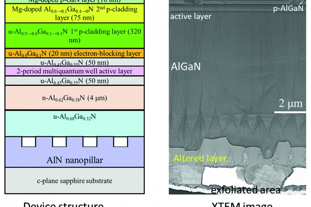
The figure above show a cross-sectional transmission electron microscopy image of the AlGaN-based heterostructure indicates that exfoliation takes place at the AlN nanopillar area.
Also critical to success is the use pressurised water. “We were not sure if this would work experimentally, so we used a household electric pressure cooker for this experiment,” revealed Iwaya, who added that they are now considering apparatus that could increase pressure, as this might speed the process.
Iwaya believes that refinements to their approach – it has already liberated 1 cm2 samples with few additional dislocations, according to transmission electron microscopy – would enable this technique to be used for volume production of AlGaN-based devices.
Currently the most time-consuming part of the process involves inserting water between the pillars. “If the viscosity of water can be reduced by increasing the void size, or by mixing it with a less viscous liquid such as alcohol, it should be possible to shorten the time required to introduce water,” argued Iwaya.
Plans for the team include: clarifying the exfoliation mechanism; increasing the diameter of exfoliation, ideally to encompass 2-inch wafers; and developing vertical UV LEDs and UV laser diodes.
“We are also looking into the production of thinner-film LEDs that can achieve a high-light-extraction efficiency, which has been applied to blue LEDs,” added Iwaya.
Reference
E. Matsubara et al. Appl. Phys. Express 15 116502 (2022)


