
ICMBE: Showcasing MBE’s credentials for high-volume production
Whilst MBE may be renowned as the best tool for growing research
samples, it has another string to its bow: it is the preferred technique
for manufacturing of a number of different devices.
BY RICHARD STEVENSON, EDITOR, CS MAGAZINE
We all make generalisations. At times we’ll get pulled up on this, with those around us pointing out examples of outliers and picking holes in our arguments. But despite this admonishment, we will soon revert to our old ways. After all, when trying to make plans and draw conclusions, spending too much time considering the cases that don’t fit in makes it nigh-on impossible to construct a line of reasoning.
It’s probably for this reason that some of us will categorise the growth techniques in our industry in an overly simplistic way. Many of us may view MOCVD as the technique for high-volume production, and see MBE as the epitaxial technology for making samples for research, such as novel quaternaries and variety of electron and hole gases. But the reality is that MBE is also a tool for volume production. This point was well made by two of the plenary speakers at the most recent International Conference in MBE, held in Sheffield, UK, from 5-9 September.
MBE for epiwafers…
Speaking at this conference – the latest in a series that dates back as far as 1978, when the inaugural meeting was held in Paris – IQE’s Amy Liu championed the diverse use of MBE for producing a variety of compound semiconductor epiwafers.
Liu, Vice President of IQE’s US R&D Programmes, kicked off her talk by pointing out that MBE has a strong track record in producing devices, dating back many decades. Early successes include the fabrication of a GaAs laser at Bell Labs in 1972.

Morris dancers provided entertainment at the ICMBE conference dinner,
held at The Cutlers Hall, Sheffield. This narrow Georgian three-storeyed
building is home to a collection of knives made from steel, an
important material for making MBE tools. Credit: Laure Divisia.
The US is also the birthplace of the world’s first MBE epi-foundry, Quantum Epitaxial Design. Launched in 1988, this trailblazing firm merged with UK-based Epitaxial Products International in 1999 to form IQE, today’s multinational powerhouse for the production of epiwafers.
IQE currently has two sites in the US with MBE capability. There’s the facility in Bethlehem, Pennsylvania, where Quantum Epitaxial Design was born; and the former RFMD facility in Greensboro, North Carolina. Consolidation is in the pipeline, involving the relocation of MBE tools at Bethlehem that are used to make a variety of infrared and III-V-on-silicon structures to the Greensboro facility, which produces GaAs wireless and photonics epiwafers.
Liu remarked that initially shipments for making GaAs-based wireless devices, such as pHEMTs, dominated the market for MBE epiwafers. However, she expects that over the coming years this market will become more diverse.
To drive down costs and boost productivity, IQE employs MBE reactors that can accommodate multiple wafers. These growth tools can house as many as 23 wafers with a 75 mm diameter, or 9 with a 100 mm diameter. Following growth, epiwafers are scrutinised by what Liu refers to as a “full suite of material characterisation tools”.
The two types of epiwafer that have been manufactured in the largest volume for the wireless sector are those for making pHEMTs and HBTs. While pHEMTs are no longer deployed in handsets in the volumes of yesteryear, HBTs are still widely used in mobile devices for amplifying RF signals, maintaining this sector’s position as the killer RF application.
With volume production at IQE dating back decades, it’s no surprise that engineers have established very mature processes on well-used tools. Liu described growth on a 7 x 150 mm platform, where 6300 runs yielded 44,000 epiwafers.
Volumes for IQE’s photonic products are smaller than those for GaAs wireless, but still significant. Like that for GaAs products, production incorporates statistical process control, but with growth typically on smaller substrates. For example, 75 mm substrates are used for making epiwafers for InGaAs photodetectors. The company’s technology portfolio also includes the production of epiwafers for InP-based edge-emitters spanning 2.1 - 2.4 µm, with good uniformity claimed on 100 mm substrates; and GaSb photodetectors, which have seen a sharp increase in demand over the last few years, according to Liu.
US department of Defense programmes have helped our industry to increase the maturity of GaSb-based devices, via efforts to increase the size of the substrate. Thanks to this, GaSb substrates initially expanded in size from 50 mm to 75 mm and then on to 100 mm. Now epiwafer production by MBE can even take place on a 7 by 125 mm platen.

ICMBE’s conference chair, David Ritchie, is Professor of
Experimental Physics at the University of Cambridge, and Professor of
Semiconductor Science and Technology at Swansea University. Credit:
Laure Divisia.
Liu shared device data for GaSb-based epiwafer production at both the Bethlehem and Greensboro sites. Evaluating material with a Surfscan 6220 revealed that all the epaiwafers are free from major defects, with defect densities well below the specified requirement. The growth process is said to be good, reproducible, and offering good control, with run-to-run repeatability.
As well as producing wafers for single-band detection, IQE is starting to make variants with dual-band detection. As one might expect, volumes for the latter are lower.
Liu also outlined plans for the future, discussing what is in the company’s pipeline, and which technologies have near-term potential. For the development of new materials and processes, IQE now uses reactors with high-volume capability from the outset. Illustrating this point, Liu mentioned that such efforts will involve high-capacity effusion cells, such as 10kg sources for indium and gallium.
One epiwafer technology that IQE is developing is that for dilute nitride lasers. Introducing this novel material allows an increase in the emission wavelength to around 1600 nm, for lasers lattice matched to either GaAs or germanium. Emitters in this spectral domain, in either the form of the VCSEL or the edge-emitter, could be deployed for sensing functions in smartphones, because emission is transparent to the OLED display. While MOCVD is the traditional workhorse for making GaAs-based lasers, particularly VCSELs, growth of the active region is found to be more successful by MBE.
IQE is active in the development of antimonide-based detectors on silicon substrates. Engineers have evaluated the quality of appropriate heterostructures on silicon, germanium-on-silicon templates and GaSb. While there are differences in defect density, values for quantum efficiency are similar. Supporting this finding is work with QmagiQ, a designer and manufacturer of infrared focal plane arrays for imaging. It has found that the performance is almost identical for all three types of substrate.

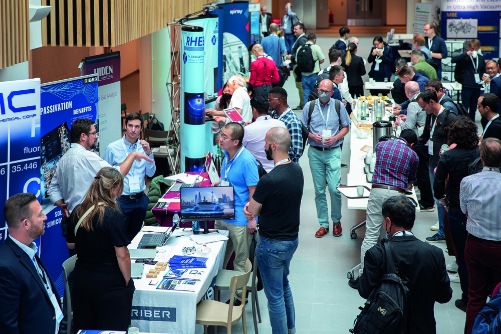
User group meetings were a feature of ICMBE. A jazz band played at
Riber’s evening, held at the student union building at the University of
Sheffield. Credit: Laure Divisia.
…and quantum-dot lasers
Delegates at ICMBE also got to hear from the Japanese firm QD Laser, a company with a tremendously strong pedigree in the production of quantum-dot lasers.
Speaking on behalf of this pioneer, company Technical Director Kenichi Nishi began his talk by acknowledging the significant contribution made to self-assembled quantum-dot lasers by one of the father’s of MBE, Arthur Gossard, who passed away this July.
Nishi went on to list some of the key attributes of the quantum-dot laser: a low threshold current; low power consumption; minimal temperature sensitivity; high efficiency; a capability to operate at high temperatures; and tolerance to back reflection.
These attributes have motivated the development of this source, first proposed by Yasuhiko Arakawa and Horroyuki Sakaki from the University of Tokyo in 1982. Converting this idea into real devices came in the 1990s, led by the group of Nikolay Ledentsov, at the time at the A. F. Ioffe Physicotechnical Institute of Russian Academy of Sciences, but now CEO of VI Systems.
Another key milestone in the history of the quantum dot laser came in 2006, when Fujitsu span out Nishi’s company, QD Laser, which makes quantum-dot lasers and other varieties of laser. According to Nishsi, the company’s core technologies are: the GaAs-based epitaxy of quantum dots and quantum wells, the fabrication of gratings employing distributed Bragg reflectors, and chip testing. Products are manufactured using a standard solid-source Riber MBE 49 reactor, capable of accommodating up to five 75 mm GaAs substrates. Material from this tool is processed into quantum-dot lasers emitting at around 1.3 μm, and InGaAs quantum well lasers spanning 1000 - 1160 nm. Nishi explained that the company’s quantum-dot lasers are produced using the Stranski-Krastanov growth mode. Today’s dots are typically around 20 nm in diameter, 7 nm high, and have a density of around 6 x 1010 cm-2.
As the morphology of the quantum dots is very sensitive to pressure, temperature and growth rate, it is essential to eliminate fluctuations during production campaigns. Helping to do this is the decision to undertake maintenance on the reactor before it fails.
Over the years, engineers at QD Laser have refined the growth of their dots. Initially these nanostructures, with a density of around 3 x 1010 cm-2, would produce a spectral peak with a width of about 35 meV and provide a gain of 25-30. Improvement first came from doubling dot density – this increased gain to 40-50. More recently, gain has been raised to 50-60 and the spectral width narrowed to around 25 meV, with refinements realised through optimised overgrowth and a suppression of diffusion, verified by bright-field transmission electron microscopy.
Since 2011, QD Laser has mass-produced lasers for optical communications, beginning with the shipment of Fabry-Pérot lasers. It has now shipped more than 4.5 million devices with a quantum-dot active region. For those lasers, temperature stability is very high, with no change in the eye diagram between 25 °C and 85 °C. Reliability is excellent, with no sudden deaths, while lifetime is estimated to be in excess of 300,000 hours. High-temperature operation is incredibly impressive, with quantum-dot Fabry-Pérot lasers capable of operation up to 220 °C and siblings with a distributed Bragg reflector able to produce single-mode lasing up to 150 °C.
Nishi argued that one of the most promising applications for the quantum-dot laser is to provide a source for optical interconnects in data centres, where they can enable high-speed transmission with a small footprint. Additional opportunities include the light source for silicon photonics and lidar.
Helping to support an expansion in the number of quantum-dot sources is IQE, which is developing epiwafers for this class of laser. One option is growth on 150 mm GaAs wafers, an approach where this epiwafer provider has demonstrated a quantum dot density of 5 x 1010 cm-2; it has also investigated the opportunity for fabrication on silicon substrates, which offer large wafer sizes, such as 300 mm, and CMOS compatibility.
According to Liu, the growth on III-V dots on silicon has seen “lots of progress” in the last few years. To drive further development, IQE has teamed up with John Bowers’ group at the University of California, Santa Barbara. This collaboration, involving the production of heterostructures with a Veeco GEN2000 reactor, has led to the fabrication of lasers with a continuous-wave output power of 125 mW.
There are also efforts at improving the performance of quantum-dot lasers at the University of Kassel and University College London. Representatives of both groups spoke at the recent ICMBE conference, highlighting that while MBE remains a great tool for producing samples for university research, it is also being used for academic efforts at developing real-world devices. Such efforts are sure to support tomorrow’s high-volume manufacture of several devices by MBE within the compound semiconductor industry.
Main Picture Credit: Laure Divisia.


