
Riber deploys MBE to support quantum computing materials
Through EPICENTRE, a Joint Laboratory with LAAS-CNRS in Toulouse, set up in June 2021, MBE company Riber has started to deploy the technologies making it possible to build the core components of future-generation quantum computers.
Quantum computers arebased on the physical phenomenon of quantum entanglement, which occurs when two elementary particles - two electrons (electrical particles) or two photons (light particles) - share identical parameters even though they are very far apart.
This requires stringent conditions for their production environment, which must be ultra-pure, ultra-controlled and ultra-cold, with single-atom precision.
The technologies available to deliver these performance levels include MBE, the material growth technique in which Riber has built up industry-leading expertise, which is one of the best positioned. That is why Riber is part of a joint quantum computers laboratory program to develop the technological components enabling them to be built.
To produce electrons or photons, it is possible to use quantum dot, small volumes of ultra-pure and ultra-controlled compound semiconductors developed and controlled using MBE. To transport them, superconductor metals can be used with ultra-precise dimensions (atomic scale), within which the electrons flow undisrupted. The MBE technology is perfect for depositing these superconducting materials in an ultra-pure environment with atomic layer-controlled thickness.
These quantum dots and superconductors need to be perfectly insulated from their environment, which is achieved by depositing dedicated oxide materials.
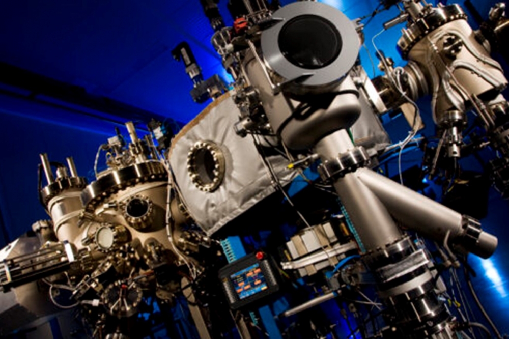
The various stages for developing the quantum dots, superconductors and insulators require various deposition chambers which must have an ultra-high - or almost perfect - vacuum in order to avoid any contamination. Vacuum quality is part of the excellence provided by Riber’s technology for these MBE machines.
An MBE machine for quantum computers will therefore include several deposition chambers connected together by robots under ultra-high vacuum conditions. It may include three to five chambers linked by two or three robots under ultra-high vacuum conditions, controlled by highly sophisticated supervision software which manages the sample movements and material deposition process.
With the complexity of this type of equipment due to the number of chambers and the ultra-purity, ultra-control and ultra-cold performance levels, this advanced technology has a market value of several million euros per machine.
This is illustrated by the order announced on October 25 for several million euros of research equipment, including several chambers and equipment items, in order to provide a new European research laboratory with the flexibility and versatility of MBE to use materials representing future quantum computer components.
Michel Picault, chairman of Riber’s executive board, concludes: “The quantum technology is very promising, but it still needs to overcome some significant development challenges to build specific chips. Riber’s MBE technology will make it possible to accelerate progress towards manufacturing quantum chips on a larger scale. Our Joint Laboratory with LAAS-CNRS will help us reach this higher level of technological maturity more quickly”.


