
Intel's 'DrGaN' tech to feature at this year's IEDM
San Francisco-based IEEE conference will feature four sessions dealing with advances in power, wide bandgap, high-frequency and cryogenic devices
The 69th annual IEEE International Electron Devices Meeting (IEDM), held in San Francisco 9th-13th December, has four sessions this year dealing with advances in power, wide bandgap, high-frequency and cryogenic devices this year.
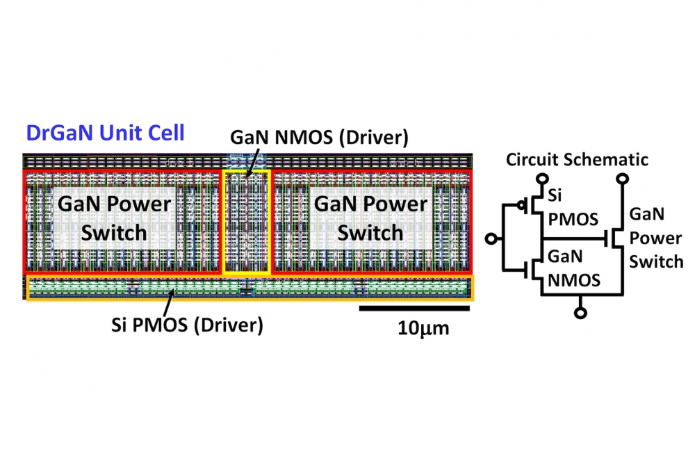
These kick off on Monday 11th December with the GaN Power Devices Integration session, which will include a paper from Intel showcasing the first CMOS 'DrGaN' technology, fabricated in a 300 mm GaN-on-Si process containing enhancement-mode GaN MOSHEMT with 3D monolithic integration of Si PMOS.
On the 12th, Recent Advances in Wide Bandgap Materials and Devices for Power Electronics, will feature six papers describing the latest work on Ga203 devices, diamond p-MOSFETs, SiC trench-etched double-implantation (TED) IGBTs, and AlSiO/p-GaN MOSFETs, from speakers including Peking University, Toyota, Nagoya University, Hitachi, Virginia Tech, and Waseda University.
High Frequency and Cryogenic RF Devices, on Wednesday the 13th, will include IBM's research on optimising InGaAS HEMT ohmic contact resistance at cryogenic temperatures, and ETH Zurich's THz characterisation of InP/GaAsSb DHBTs, demonstrating 1.46 THz fmax at 50K. Other speakers in this session include the Shanghai Institute of Microsystem and Information Technology, CEA-Leti, and KAIST.
The final session, also on the 13th, is Wide Bandgap Devices for Power and RF Applications, which will include a paper by Xidian University discussing a b-Ga2O3 RF MOSFET on a SiC substrate with 30 percent power-added efficiency and ft/fmax of 27.6/57 GHz. There will also be speakers from IMEC, CEA Leti, and Stanford University. The session concludes with an invited paper from ETH Zürich on a novel metadevice concept based on microscopic manipulation of RF electric fields, with applications within future telecoms technologies.


