
Researchers develop new way to tailor-make thin films
Rolling transfer method can produce thin organic semiconductor films automatically and with well-defined properties
A German-American team of scientists – led by Leibniz IPHT in Jena, Germany – have developed a new approach fordepositing thin organic semiconductor films automatically and with well-defined properties.
The method, presented in the journal Advanced Materials, should make it possible to produce thin films with controllable interactions between neighbouring molecules and specific energy levels.
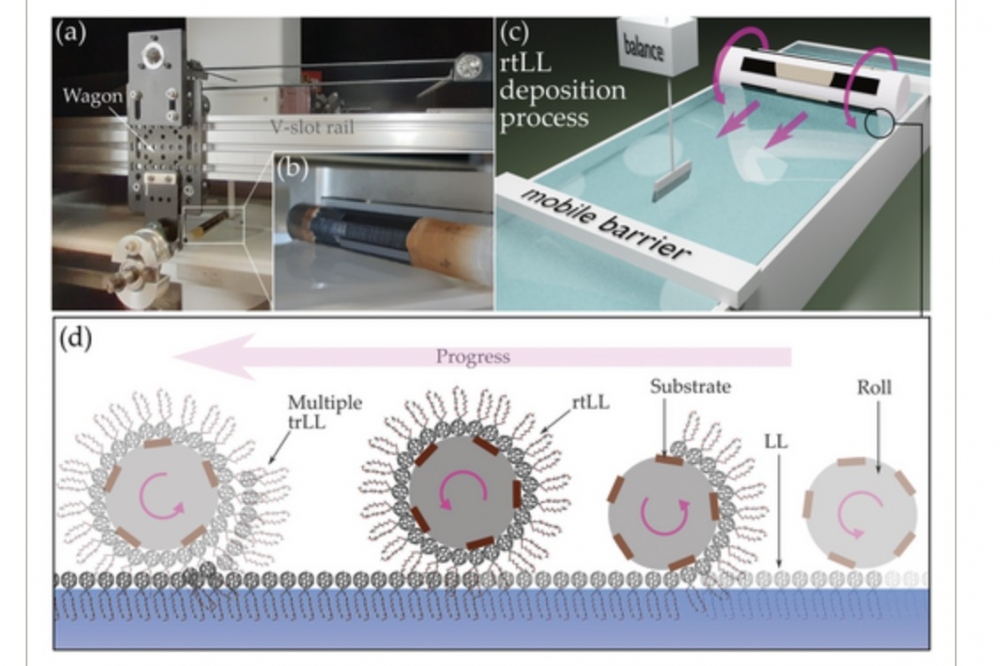
The team's 'Rolling Transfered Langmuir Layer' technique, a further development of the established Langmuir Blodgett technique for the deposition of thin films, is suitable for the production of monolayers of organic semiconductor molecules at air-water interfaces.
A layer of molecules formed on a water surface is transferred to a solid substrate. The molecular monolayer is deposited on the substrate using a specific rolling transfer system developed by the researchers, which contains the substrate to be coated and which is moved over the molecular film on the water surface. The molecular layer formed at the air-water interface adheres to the substrate during the rolling motion.
According to Martin Presselt, head of the Organic Thin Films and Interfaces Group at Leibniz IPHT, the process allows crystalline films to be deposited with minimal surface defects and to produce both monolayers and multiple thin-film layers with individual properties directly, uniformly and with high quality in a scalable manner.
The technique makes it possible to vary the packing density of the molecules within a layer, which can range from very densely packed to less densely packed, via the surface pressure during deposition. Also, the number of stacked molecular layers and thus the layer thickness of the thin films can be precisely adjusted. "In this way, semiconductor thin films with targeted interactions between neighbouring molecules and specific energy levels can be reproducibly produced," says Sarah Jasmin Finkelmeyer, a scientists in the Organic Thin Films and Interfaces Group.
The researchers say this approach lays the foundation for the fabrication of thin-film-based novel (opto-) electronic components with optimised properties. For example, organic photovoltaic modules that efficiently generate electrical energy from sunlight as well as thin films that convert sunlight into chemical energy can be further developed.
Pictured above: a) Rolling transferred Langmuir layer (rtLL) deposition setup. b) Magnified view of the role with mounted substrates. c, d) Schematic representation of the rtLL deposition process.
Reference
'Tailoring the weight of surface and intralayer edge states to control LUMO energies' by S. J. Finkelmeyer et al; Advanced Materials (2023)


