Epitaxy with a twist
DoE team finds that crystals can twist when sandwiched between two substrates
Researchers with the Department of Energy’s SLAC National Accelerator Laboratory, Stanford University and the DOE's Lawrence Berkeley National Laboratory (LBNL) grew a twisted multilayer crystal structure for the first time and measured the structure’s key properties. They think twisted structure could help researchers develop next-generation materials for solar cells, quantum computers, lasers and other devices.
“This structure is something that we have not seen before – it was a huge surprise to me,” said Yi Cui, a professor at Stanford and SLAC and paper co-author. “A new quantum electronic property could appear within this three-layer twisted structure in future experiments.”
The team believe they have extended the concept of epitaxy. To date, epitaxy research has focused on growing one layer of material onto another, and the two materials have the same crystal orientation at the interface. This approach has been successful for decades in many applications, such as transistors, LEDs, lasers and quantum devices. But to find new materials that perform even better for more demanding needs, like quantum computing, researchers are searching for other epitaxial designs – ones that might be more complex, yet better performing, hence the 'twisted epitaxy' concept demonstrated in this study.
In their experiment, detailed this month in Science, researchers added a layer of gold between two sheets of semiconducting material, MoS2. Because the top and bottom sheets were oriented differently, the gold atoms could not align with both simultaneously, which allowed the gold structure to twist.
“With only a bottom MoS2 layer, the gold is happy to align with it, so no twist happens,” said Cui. “But with two twisted MoS2 sheets, the gold isn’t sure to align with the top or bottom layer. We managed to help the gold solve its confusion and discovered a relationship between the orientation of gold and the twist angle of bilayer MoS2.”
“We’re beginning to explore whether only this combination of materials allows this or if it happens more broadly,” said Bob Sinclair, a professor in Stanford’s school of Materials Science and Engineering and paper co-author. “This discovery is opening a whole new series of experiments that we can try. We could be on our way to finding brand new material properties that we could exploit.”
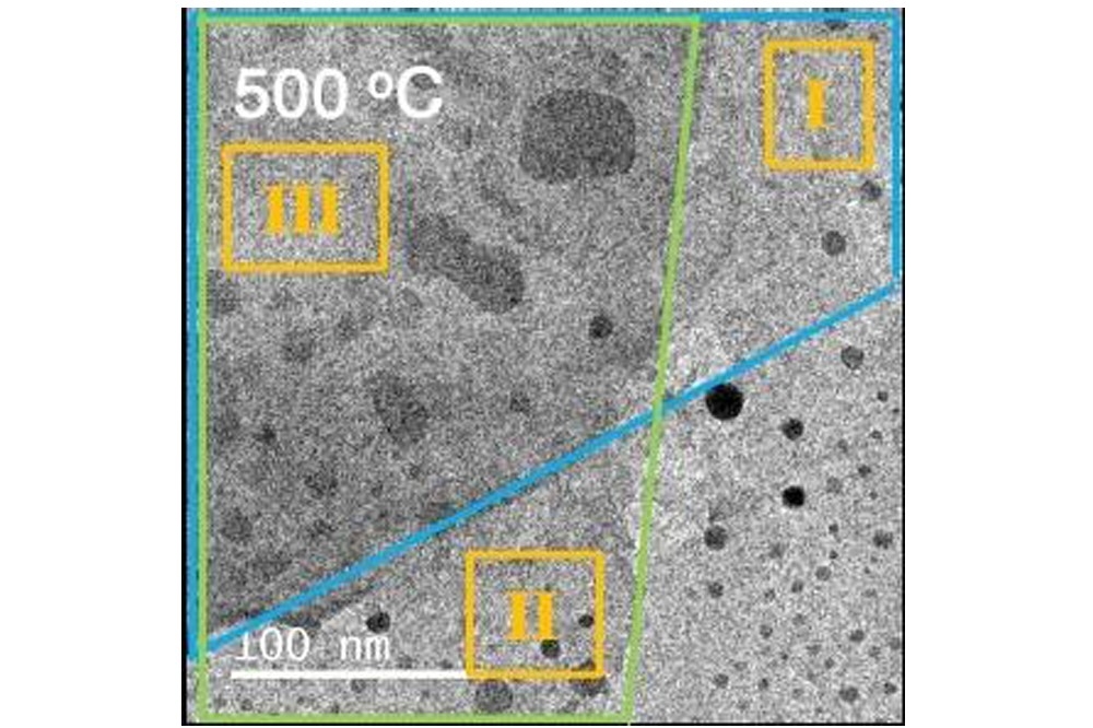
The image above shows the locations of gold nanodiscs in various experimental conditions. The MoS2 layers and gold nanodiscs together heated up to 500 degC. The three marked regions – I, II, and III – indicate the various layers of the sample. Region I shows gold on the bottom MoS2 layer; II shows Au below the top MoS2 layer; and III shows the gold between the top and bottom MoS2 layers. The gold nanodiscs are the darker regions in the region III.