A new option for monolithic multi-colour microLED arrays
Tunnel-junctions address the challenge of producing ohmic contacts on a plasma-etched p-type surface
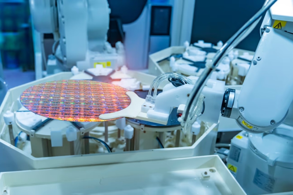
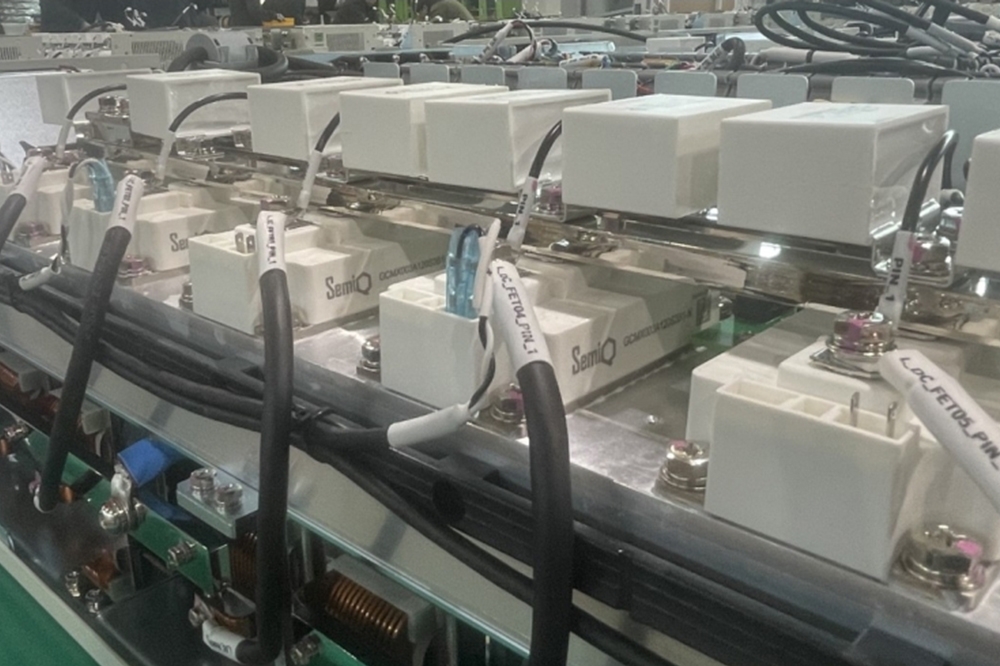
Due to yield and throughput issues associated with the pick-and-place approaches that are being pursued to produce displays based on microLEDs, monolithic technology is attracting much interest.
On that front a collaboration between engineers at Meijo University and King Abdullah University of Science and Technology (KAUST) is making substantial progress – they are claiming to have produced the first red, green and blue (RGB) monolithic microLED arrays that are GaN-based and connected via tunnel junctions.
“We have also succeeded in minimising the voltage increase due to etching damage by using tunnel junctions,” says team spokesman Motoaki Iwaya from Meijo University. “Such an approach is considered extremely effective in realising monolithic displays with microLEDs.”
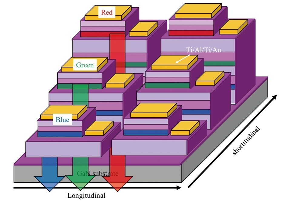
The engineers at Meijo University have produced an epistructure that includes a blue-emitting double-quantum-well region, followed by a tunnel junction, and then a green-emitting double-quantum-well region, also followed by a tunnel junction. After shipping this epistructure to KAUST, that team added a red-emitting structure, featuring a red single quantum well grown on top of a blue single quantum well to increase emission efficiency.
Several steps were employed to form microLED arrays with 330 pixels-per-inch from the epiwafer. Efforts began with the addition of ITO by sputtering, followed by inductively coupled plasma-reactive ion etching with chlorine gas to form a mesa structure. Subsequent annealing activated p-type GaN in the tunnel junctions, prior to passivation with a SiO2 layer and the addition of n-type electrodes by electron-beam deposition.
The microLEDs produced by this process have a device size of 73 µm by 20 µm, and a mesa area of 35 µm by 15 µm. However, scaling to far smaller dimensions is possible, says Iwaya, who revealed that they have realised highly efficient luminescence from a square single element with sides of about 3 µm. Iwaya added that the team is yet to have the technology to implement 3 µm devices, but once they have a mounting technology available, they hope to demonstrate displays finer than 2000 ppi.
Driven at 50 mA, the blue, green and red microLEDs in the array produce emission with peaks at 486 nm, 514 nm and 604 nm. There is also an additional, weaker peak produced by the blue microLED at 380 nm, which could be eliminated by applying AlN cap layers and lowering the growth temperature of the n-type AlGaN layer to that of the active layer of the blue LED. Another concern is what is described as broad fringe emission from the red LED, occurring at around 450 nm, possibly resulting from non-optimal growth conditions.
The turn-on voltages for the blue, green and red LEDs were 2.8 V, 3.2 V and 3.2 V. For the green and red LEDs these values are 0.5 V and 1 V higher than they would be for an ideal LED. The green microLED is thought to be held back by the anode forming an electrical barrier at the growth interface, while the red microLED may be impeded by a combination of a high contact resistance between p-type GaN and the electrode, and a small electrode area that increases contact resistance.
Optical measurements reveal that the intensity of emission from the green microLED is far higher than that from its blue and red siblings.
“For blue, it is possible to increase brightness by about one order of magnitude and control wavelengths if the effects of heat are suppressed,” says Iwaya, who anticipates that improvements to the red microLED will be much harder to realise. He accepts that it will be a challenge to produce red microLEDs that emit higher luminance at longer wavelengths. “However, luminance is already about one order of magnitude higher than that of OLED, so I think it is possible to bring it to a practical level.”
Reference
T. Saito et. al. Appl. Phys. Express 16 084001 (2023)