The growth of MBE
With ramping sales of production tools and emerging longer-term
opportunities, Riber’s revenue is set to stay on an upward trajectory.
BY RICHARD STEVENSON, EDITOR, CS MAGAZINE
Within our community, it’s often said that MOCVD is the tool of choice for epitaxial growth in high-volume fabs, while MBE is the preferred technique for the academic researcher. But the reality is far more nuanced. While it is true that MOCVD dominates chip production, sales of MBE tools to makers of compound semiconductor devices are rising, and will continue to do so.
It is a trend that is helping to swell sales at Riber, the French producer of a wide portfolio of MBE tools. Annual sales of the company’s epitaxial systems climbed by 96 percent between 2022 and 2023 to hit €29.0 million, and total revenue for this year is expected to surpass last year’s €39.2 million, which included €10.3 million for services and accessories.
According to the company’s CEO, Annie Geoffroy, Riber’s success stems from both a rise in its global sales of MBE tools, and an increase in its market share.
Accounting for almost two-thirds of Riber’s 2023 revenue are sales to Asia. This success, so far from the company’s head-quarters on the outskirts of Paris, is attributed to establishing local support for its customers. Such efforts have been up and running for 12 years, and have helped Riber win overseas business and strengthen its relationship with its customers.
Recent dealings with Asian chipmakers includes an order placed this January for a pair of MBE 412 systems for device development, and an MBE 6000 that will be employed to increase the production of GaAs pHEMTs.
Despite this device being replaced by silicon-on-insulator technology in the majority of smartphones, it is still being produced in volume worldwide.
“Some customers in the US are still making pHEMTs,” reveals Riber’s marketing manager Claudine Payen, who believes that these transistors may have specific requirements that demand growth by MBE.
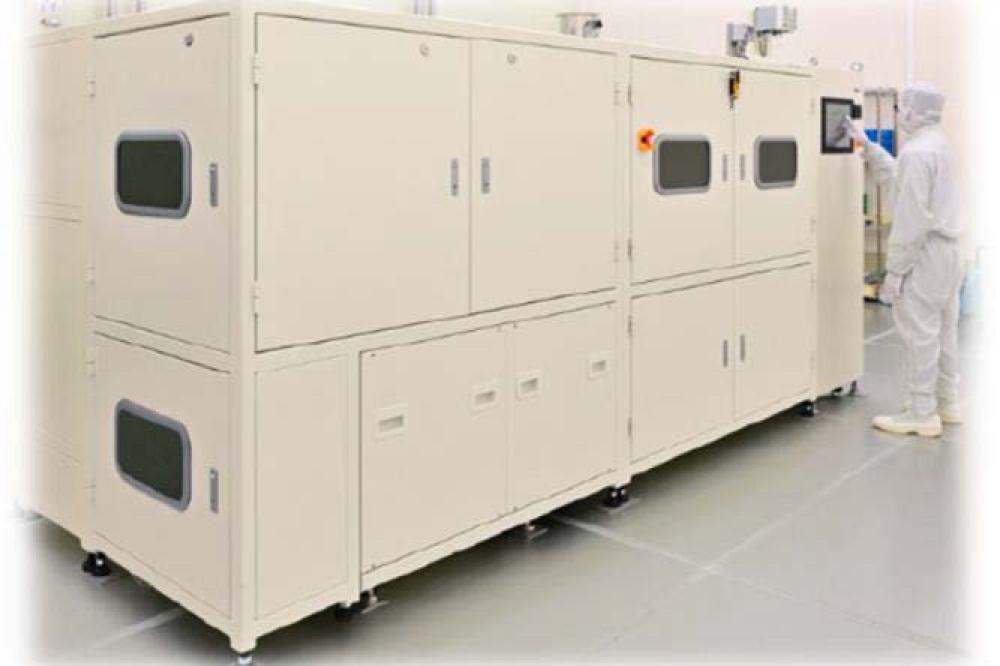
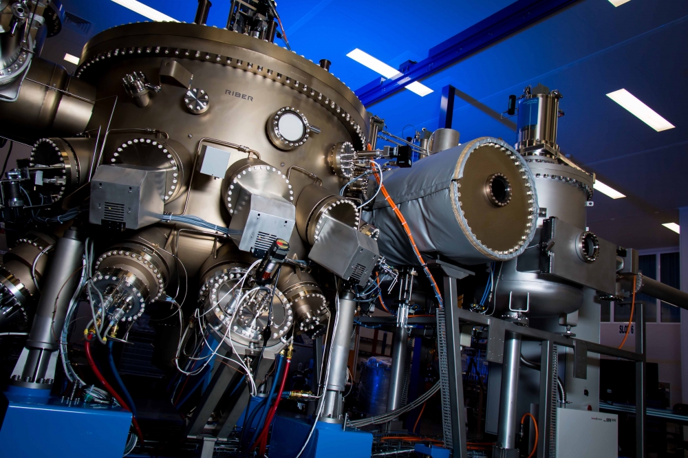
Another industrial market for Riber is that of the VCSEL. Interest in increasing the production efficiency of this form of laser has led the French outfit to develop a new tool, the Riber MBE 8000, in collaboration with US epiwafer provider Intellepi.
“We worked on the design of the 8000 to have a big capacity and also very, very good uniformities,” says Payen. She explains that this tool, capable of accommodating four 200 mm wafers, can also be used for other epitaxial designs demanding excellent layers, very tight interfaces, and a high degree of thickness and compositional uniformity.
According to company CTO, Jean-Louis Guyaux, there is a lot of interest in Riber’s tools for the growth of InP avalanche photodiodes, as well as GaN-based LEDs emitting in the UVC. For the later, a new pilot line has been established that features a Riber MBE 49, a tool that can be used for growth on a single 200 mm wafer, or for multiple 100 mm wafers.
Over the last two-to-three years, Riber has also drawn on MBE to develop a technique for the passivation of laser bars, coating them with ZnSe. The company’s completely automated tools carry out this task under vacuum in high-volume fabs.
Another of Riber’s diversifications is the pursuit of MBE within the silicon industry. The established electro-optical modulators using p-n junctions formed from silicon are encroaching their performance limit, and gains can be realised by turning to functional oxides, such as BaTiO3, argues Guyaux. He adds: “It's pushed, of course, by the current datacom silicon market, but there is a lot of interest there for quantum computing with photons.”
Stalwart systems
Due to the long lifetime of MBE systems, most orders are placed to increase capacity, rather than replace an older tool. As the growth chamber is made from stainless steel, it could last forever with regular maintenance and the replacement of parts.
“The obsolescence is coming mainly from the electronics,” says Guyaux, who explains that the servicing of production tools may include upgrading electronics and control software, and introducing new in-situ, real-time instruments.
Within academia, it’s not uncommon for epitaxial growth to be undertaken in tools dating back to the 1980s. However, Riber still nets orders for new tools for universities, often when new research projects win funding that includes an allocation for purchasing a new growth tool.
“There's also this matter of size,” says Payen, who points out that legacy equipment may only accommodate very small wafers, while projects need to demonstrate processes on larger wafers.
One of the company’s goals for 2024 is to advance the proven capabilities of its MBE 8000.
Another is to continue its work on a project called ROSIE, short for Riber Oxide Silicon Epitaxy, involving the development of this growth technology for 300 mm wafers. Guyaux sees such efforts as crucial to the evolution of the semiconductor industry. He forecasts a future beyond III-V fabs, silicon fabs, and the subsequent marriage of these two technologies. Silicon will be the only technological platform to survive, due to its capability to address very large markets, but III-Vs and SiC will be added to this foundation.
“This is where MBE has a real advantage, due to its thermal budget,” claims Guyaux. He points out that with MOCVD, the high temperatures needed to crack the precursors threaten to damage the wafer, an issue that may be avoided by MBE growth.
Another fundamental change to the compound semiconductor industry could be the development of hybrid epitaxial tools that combine MBE with other growth technologies.
Riber is working on this – another reason to believe that the company is well-positioned for the coming years. As well as healthy orderbook, rising sales, and an expanding portfolio of MBE tools, it is preparing for a future that is forecast to witness some major changes within our industry.
Main image: The Riber MBE 8000, the company’s flagship production tool, has been developed in collaboration with US epiwafer provider Intellepi.

