Stronger, faster, lighter
Lehigh University professor awarded $1.1M to develop ultra WBG materials for military radar
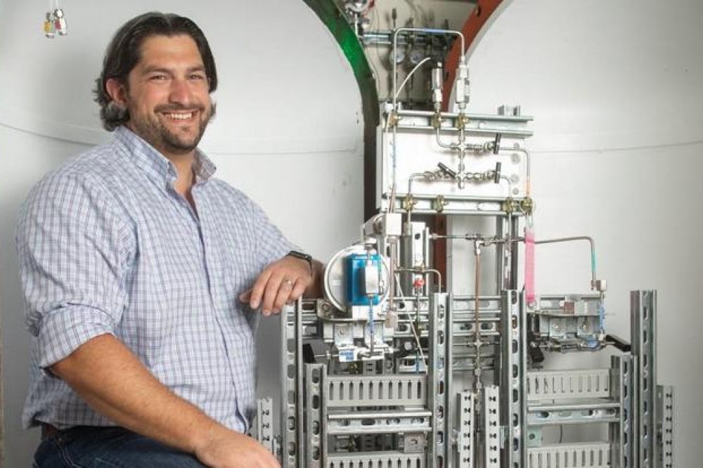
Siddha Pimputkar, assistant professor of materials science and engineering at Lehigh University, has been awarded a $1.1 million grant from the US DEVCOM Army Research Laboratory to research the development of ultra-wide band gap UWBG) semiconductor materials for use in RF.
“The Army is interested in radio frequency emitters, radar systems, that perform at higher power levels and frequencies to let them go farther into the field,” Pimputkar said. “To do that, you need better semiconductor materials.”
While wide bandage materials like GaN and SiC remain in relatively early stages of adoption, the military is already looking to benefit from materials with even higher capabilities. In 2020, the US Army Combat Capabilities Development Command/Army Research Laboratory/US Army Research Office (ARO) issued a call for proposals to develop UWBG RF electronics.
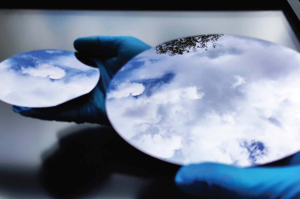
UWBG materials have bandgaps greater than GaN’s 3.4 electron volts. Members of this class include diamond, aluminum gallium nitride (Al1--xGaxN), and beta-phase gallium oxide (β-Ga2O3).
“The challenge now is, can we do even better than GaN and SiC?” Pimputkar said. “Now we’re talking about materials that used to be considered insulators, but if we can control the electron concentrations in them, we can consider them ultra-wide bandgap semiconductors.”
Exceeding diamond
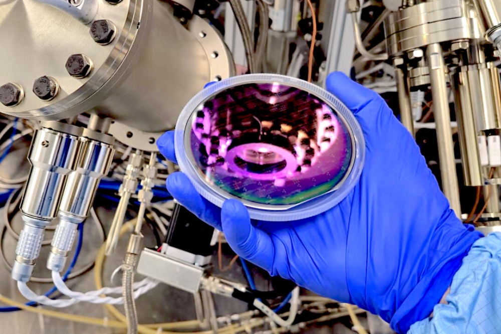
Diamond is considered by many to be the leading UWBG material for applications due to an advantageous combination of material properties. It has the potential to perform well in high-voltage and high-frequency applications, and recent advances have made it possible to grow single crystal synthetic diamonds in laboratory settings.
However, there are challenges to using diamond as a semiconductor material, including difficulties in doping the material for some applications.
Pimputkar believes that cubic Boron Nitride (c-BN), holds the greatest potential for power electronic applications. The compound’s atoms are arranged in a structure similar to that of diamond and the material has a wider bandgap of 6.4 eV compared to 5.5 eV for diamond.
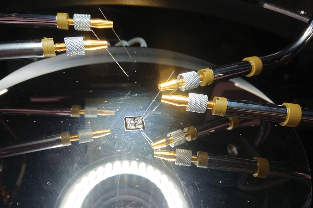
But c-BN comes with challenges of its own—namely, growing it at crystal sizes needed to produce wafers
Currently, the process for growing bulk, single crystal c-BN is similar to that of synthesizing diamonds, requiring high pressures and high temperatures while yielding crystals only millimetres in size.
“For electronics, you need crystals of centimeters or inches to create wafers,” Pimputkar said. “I want to find a way to grow c-BN using a process that actually scales to an industrial level.”
The path there is two-pronged. One goal is to grow c-BN using a new process that requires less pressure. The other is to grow it large enough to make a device enabling the measurement of the saturation velocity of electrons in c-BN, something that has been done so far only using computational methods.
“Based on figures of merit, c-BN is the best,” he said. “Now, can we make a c-BN device that can substantiate the promised properties of the material? No one has been successful in doing that yet.”
Pimputkar theorises that the process of growing c-BN at lower pressures can be enabled by beginning with a seed crystal of c-BN and depositing more boron nitride onto its surface using a new synthesis pathway and appropriate catalysts. He believes this method can produce the desired cubic crystal structure and not just the more readily grown hexagonal structure.
“While hexagonal boron nitride (h-BN) is a fantastic material in its own right, we are learning how to coax out the cubic version,” he said.
Pimputkar’s lab has established expertise in researching nitride growth processes under his prior NSF CAREER grant. The lab has been investigating the c-BN growth question for approximately a year and a half, roughly halfway through the initial three-year US Army grant period, which could be extended up to two additional years.
“We’re at a phase where we are trying to understand what it takes to grow c-BN instead of h-BN,” he said. “We’re aiming for a proof of concept followed by demonstration of cm-scale crystals we can give people to further test it for its future potential. It’s high-risk, high-reward.”