Argonne National Lab gets $4M to develop MoS2 chips
US Lab to collaborate with multiple universities to advance new 2D materials
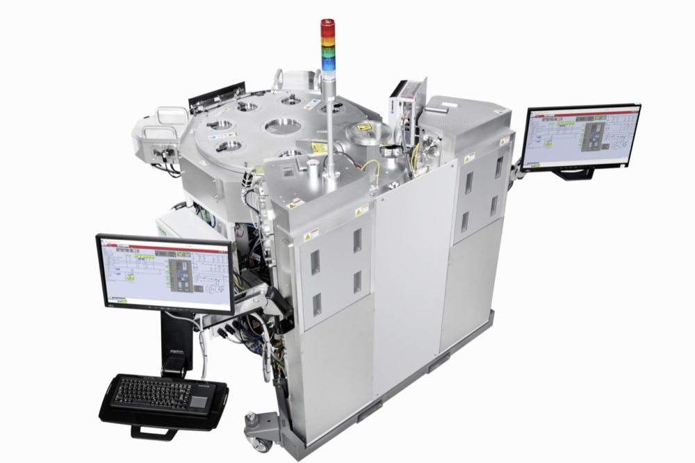
The US Department of Energy (DOE) has awarded DOE’s Argonne National Laboratory $4million to fund research that will use atomic layer deposition (ALD) to advance 2D materials and devices for creating microchips that use up to 50 times less energy than current chips.
Set to launch in early 2024, the two and half year project is funded by the Energy Efficient Scaling for Two Decades (EES2) program of the DOE’s Advanced Materials and Manufacturing Technologies Office. It focuses on the 2D compound semiconductor MoS2.
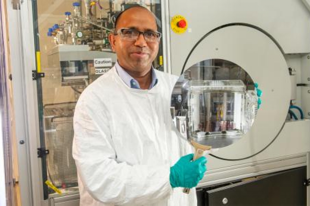
Argonne will partner with Stanford University, Northwestern University and Boise State University on the project. Argonne Distinguished Fellow Jeffrey Elam (pictured above), who founded and directs Argonne’s ALD research program, will lead the research team.
“Computers today spend over 90 percent of their energy shuttling data back-and-forth between the memory and logic functions, which exist on separate chips,” Elam said. “This limitation is known as the ‘von Neumann bottleneck.’ Energy used to move the data is wasted as heat. As computing demand grows, we must develop low-power transistors and microchips to overcome this bottleneck and prevent an energy crisis.”
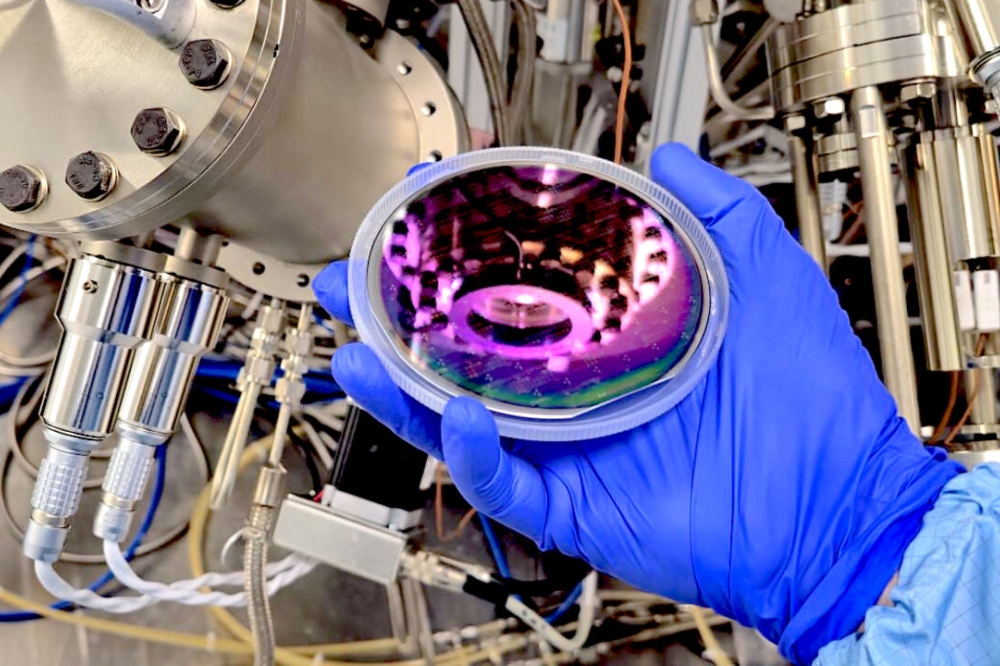
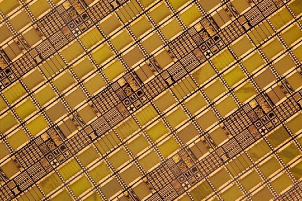
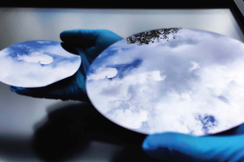
Building on previous research, Argonne scientists are using ALD to create atomically precise MoS2 films. “We can create extremely thin, 2D MoS2 sheets. These sheets will replace the bulky, 3D silicon thin films used in today’s transistors. This leaves more room on the microchip to effectively stack the memory and logic together, dramatically reducing energy,” Elam said.
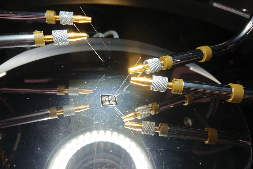
Argonne, in collaboration with Boise State University, developed ALD methods for creating 2D MoS2 films. The team will demonstrate the use of MoS2 to create 2D-FETs that can be stacked in 3D. This method allows the integration of memory and logic functions not possible with silicon.
Simultaneously, Argonne scientists are demonstrating the use of ALD MoS2 in memtransistors, electronic components used to build neuromorphic circuits. This technology is relatively new. But neuromorphic circuits have the potential to use one million times less energy compared to conventional silicon devices.
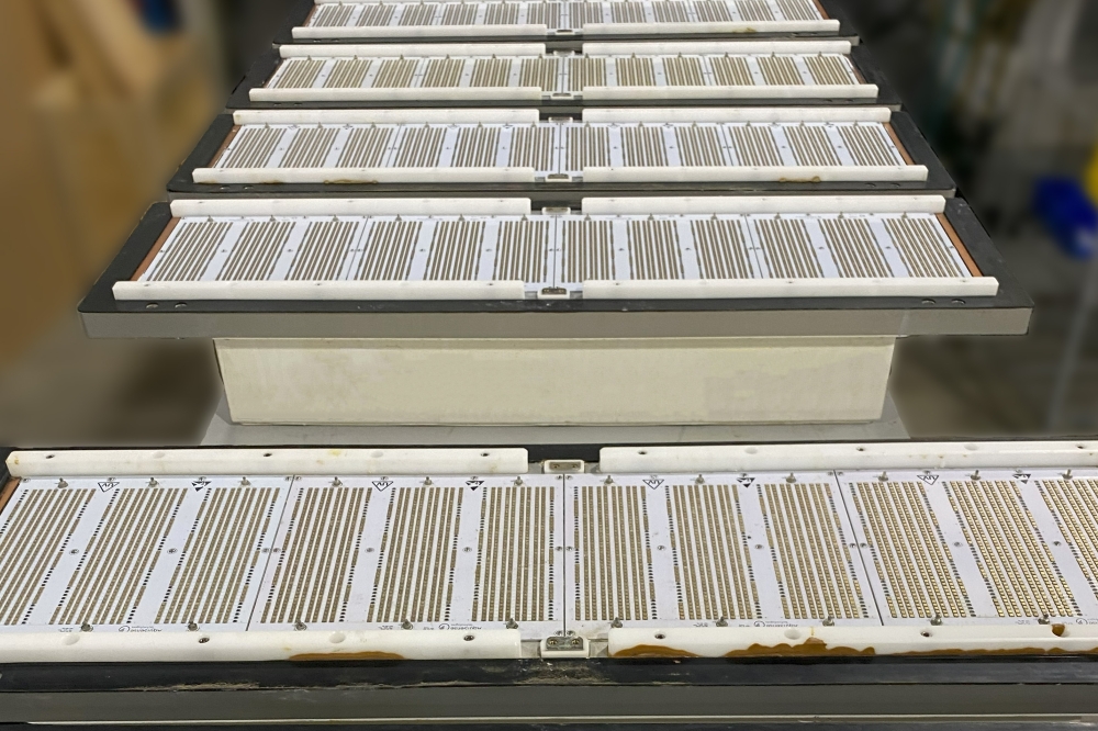
Both 2D-FETs and memtransitors have been successfully demonstrated at the lab scale by growing MoS2 at high temperatures. Argonne scientists want to take the technology to the next level. Commercial manufacturing will require MoS2 to be deposited on large, pizza-sized wafers at low temperatures. In this DOE project, the research team will develop these capabilities to ensure that the MoS2 ALD is compatible with current semiconductor manufacturing processes.