PhotonixFAB opens for prototyping

EU-funded fab initiative opens customer portal for early technology access
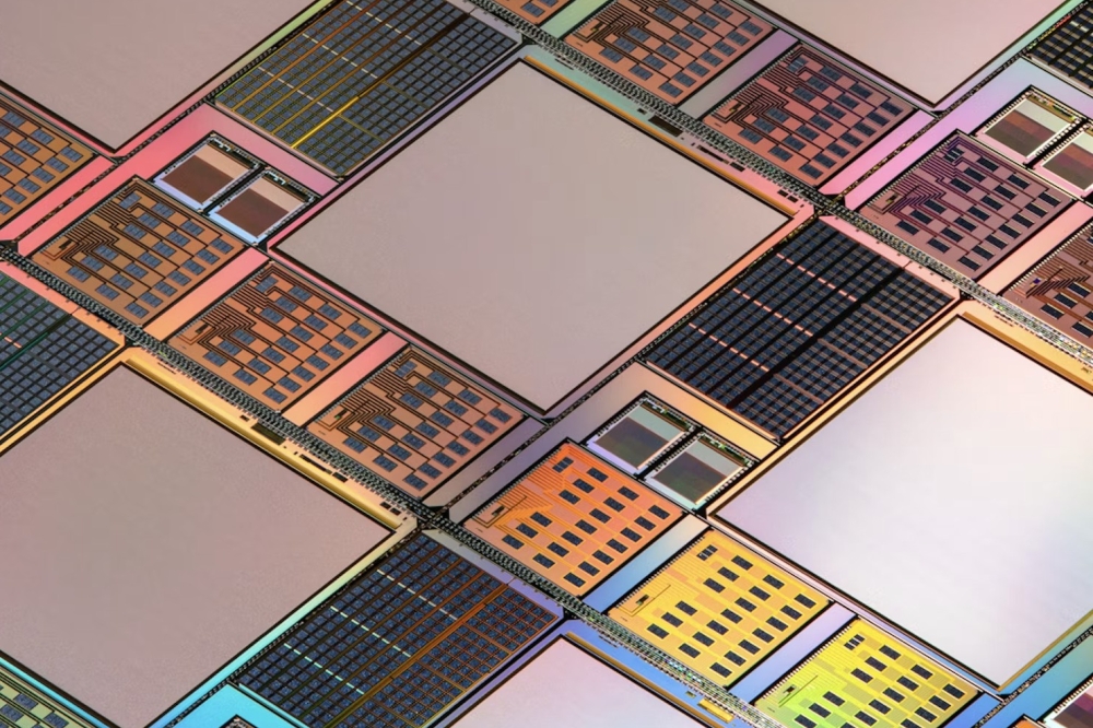
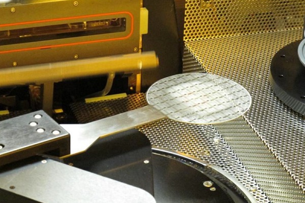
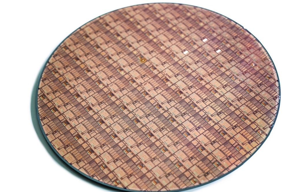
Consortium partners of the European Union (EU) funded PhotonixFAB initiative have taken the first step to industrialise the European silicon photonics value chain by providing early access to R&D and small-scale manufacturing with a customer engagement portal.
Announced in mid-2023, PhotonixFAB aims to elevate Europe's standing in silicon photonics. The initiative draws together the continent’s most innovative enterprises within the photonics sector (each supplying their own specific proficiencies), along with respected research establishments.
The customer engagement portal will enable initial technology evaluations and consultations, and allow customers to learn about the different capabilities offered by the respective members of the PhotonixFAB consortium.
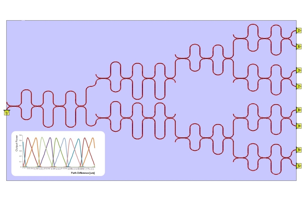
Examples of the capabilities that customers can initiate will include prototyping in relation to SiN via LIGENTEC and SOI through Imec, as well as for InP chiplets by working with SMART Photonics. There will also be the packaging expertise that PHIX Photonics Assembly offers for both SiN and SOI processes, plus early technology access for InP micro-transfer printing on SiN/SOI supplied directly by X-FAB and supported by SMART. PDKs based on Luceda’s EDA tool are available through the technology partners.
”We are seeing a great deal of interest in the European-based silicon photonics value chain that PhotonixFAB represents. This launch signifies that we are now open for business and projects can get underway, so no time is wasted. It means that we can accelerate engagement activity and customers can get ahead of the game,” adds Joni Mellin, business line manager for Photonics at X-FAB.

