Argonne Lab to lead MoS2 chip project
$4M collaborative US Department of Energy project to advance 2D semiconductors and devices for next-generation microchips
Predictions indicate that 20 percent of the world’s energy could be consumed by microelectronics by 2030. Averting this crisis hinges on developing new transistors.
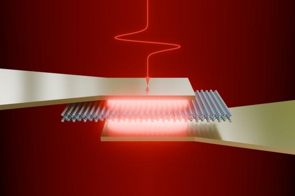
Now the US Department of Energy (DOE) has awarded DOE’s Argonne National Laboratory $4 million to fund research that will use atomic layer deposition (ALD) to demonstrate the use of MoS2 to create tiny 2D-FETs that can be stacked in 3D.
The researchers think such chips would use up to 50 times less energy than current ones.
Set to launch in 2024, the project — which will last two and a half years — is funded by the Energy Efficient Scaling for Two Decades (EES2) program. Argonne will partner with Stanford University, Northwestern University and Boise State University on the project. Argonne Distinguished Fellow Jeffrey Elam, who founded and directs Argonne’s groundbreaking ALD research program, will lead the research team.
“It is only recently that microelectronics started using a large fraction of the Earth’s electricity,” said Elam. “Computers today spend over 90 percent of their energy shuttling data back-and-forth between the memory and logic functions, which exist on separate chips,” Elam said. "Energy used to move the data is wasted as heat. As computing demand grows, we must develop low-power transistors and microchips to overcome this bottleneck and prevent an energy crisis.”
In this project, Argonne scientists will use ALD to redesign the microchip around 2D MoS2 s in an attempt to eliminate the back-and-forth shuffling of data. “We can create extremely thin, 2D MoS2 sheets. These sheets will replace the bulky, 3D silicon thin films used in today’s transistors. This leaves more room on the microchip to effectively stack the memory and logic together, dramatically reducing energy,” Elam said.
Simultaneously, Argonne scientists are demonstrating the use of ALD MoS2 in memtransistors used to build neuromorphic circuits. This technology is relatively new, but such circuits have the potential to use one million times less energy compared to conventional silicon devices.
Both 2D-FETs and memtransitors have been successfully demonstrated at the lab scale by growing MoS2 at high temperatures. Argonne scientists want to take the technology to the next level. Commercial manufacturing will require MoS2 to be deposited on large wafers at low temperatures. In this DOE project, the research team will develop these capabilities to ensure that the MoS2 ALD is compatible with current semiconductor manufacturing processes.
Scientists at the partner institutions will use their expertise to advance specific areas of the project. Eric Pop at Stanford University will develop 2D-FET devices, Mark Hersam at Northwestern University will develop memtransistors that use the ALD MoS2, and Elton Graugnard at Boise State University will perform advanced characterisation of the ALD MoS2 coatings to evaluate the quality of materials.
In parallel with the experimental work, Argonne is using modeling and simulation to design energy-efficient devices that incorporate ALD MoS2. Researchers aim to advance the stacked devices toward a pilot-scale demonstration, with the goal of marketing them for commercial use.
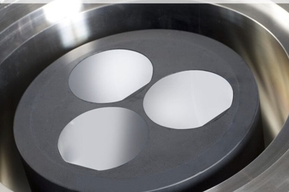
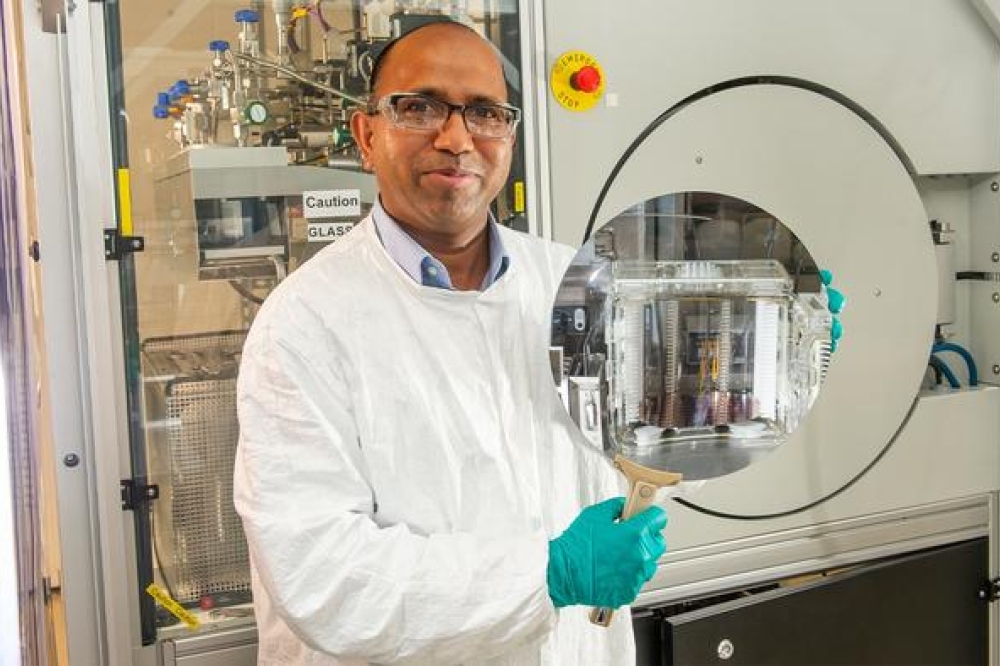
Pictured above: Argonne Senior Scientist Anil Mane holds a 300 mm silicon wafer coated by ALD using the instrument in the background. (Image by Argonne National Laboratory.)