Gate to the future
Reliability benefits from deploying deposited gate oxides in SiC MOSFETs.
BY ARNE BENJAMIN RENZ, PETER GAMMON, OLIVER VAVASOUR, VISHAL SHAH AND MARC WALKER FROM THE UNIVERSITY OF WARWICK, SUPPORTED BY JAMES GOTT FROM WARWICK MANUFACTURING GROUP AND ANDREW NEWTON AND MICHAEL POWELL FROM OXFORD INSTRUMENTS PLASMA TECHNOLOGY
The potential of wide bandgap power devices to deliver efficient, compact and light power conversion has been known since the 1980s. However, it was not until the late 2010s that the first SiC power converters from Tesla, BYD, Hyundai and others demonstrated the reliability and viability of the material for mass adoption. In the wide bandgap boom that followed, numerous press releases from OEMs and IDMs announced SiC chip supply agreements and joint ventures. In turn, multiple SiC IDMs have announced major billion-dollar expansion plans and supply agreements from SiC substrate manufacturers. The result is an industry that is predicted by Yole to reach $8.9 billion in 2028 at an average compound annual growth rate of 31 percent.

Figure 1. Individual series resistance contributions to total specific on-resistance in 650 V and 1200 V planar MOSFETs.
With a SiC MOSFET based inverter expected to be 5 percent more efficient than a silicon IGBT equivalent, the fact that the SiC chips can be up to three times more expensive is more than compensated for by the potential battery reduction. However, as OEMs become more familiar with the technology, and competition between SiC IDMs mount, so the pressure for cost reductions increase. This is fuelling the development and adoption of 200 mm diameter substrates, the move to automated fabrication, and a move to reuse substrates.
However, many of the tools of cost reduction sit with the device designer, for whom every milliohm of resistance in their design contributes to the size of the finished die. By minimising the specific resistance of a die, a given product will be smaller, in turn increasing yields. As such each of the yields shown in Figure 1 need to be minimised, including the MOSFET channel, which is the subject of this work.

Figure 2. (left) Cross-sectional image emphasising the individual
resistance contributions and (middle and right) an image of a packaged
device.
Challenges in gate structures
With up to one third of a SiC MOSFET’s resistance originating from the channel, shown in Figure 2, this is one of the dominant resistance components in 650 V or 1200 V MOSFETs for EV systems. The main reason for this highly resistive channel is the high density of defect states at the interface between the semiconductor and dielectric. For the SiO2/SiC interface, the density of interface defect states is typically between a hundred and a thousand times higher than it is for SiO2/silicon. These unwanted states, and the charges trapped in them, enhance scattering at the interface. In turn, the increased scattering drags down channel mobility and significantly increases the channel resistance. The channel mobility in today’s commercial MOSFET applications is just 20-40 cm2 V-1 s-1, far lower than the theoretically achievable bulk mobility of SiC, which is around 1000 cm2 V-1 s-1.
Ironically, the root cause of the high channel resistance in the SiC MOSFET is related to one of its biggest strengths: unlike GaN and diamond, SiC can be thermally oxidised to form SiO2. However, the presence of carbon causes problems.

Figure 3. (Top) Interface states build-up due to incomplete carbon
transfer away from the interface and (middle) interfacial charge
scattering in the channel, causing a decrease in channel mobility;
(bottom) common post-oxidation anneals to improve channel mobilities.
During regular oxidation, occurring at temperatures of more than 1200 °C, SiO2 initially forms through the consumption of SiC, and carbon is dispersed as CO2. However, as the SiO2 get thicker, not all carbon can diffuse through it, causing carbon to accumulate at the SiC/SiO2 interface (see Figure 3). This trapped carbon creates charge states in the channel region of the SiC MOSFET that scatter electrons and impair the channel mobility of this transistor.
One option for improving channel mobility is post-oxidation annealing in NO or N2O. Alternatively, the oxide can be grown using NO or N2O directly. The origin for this improvement is disputed, but a popular and widely accepted explanation is that the nitrogen attaches itself to dangling bonds and other atomic defects, rendering them passive and inactive. Of the two sources of nitrogen, NO gives the highest channel mobility. However, as it is toxic and difficult to handle safely, N2O is often used instead.

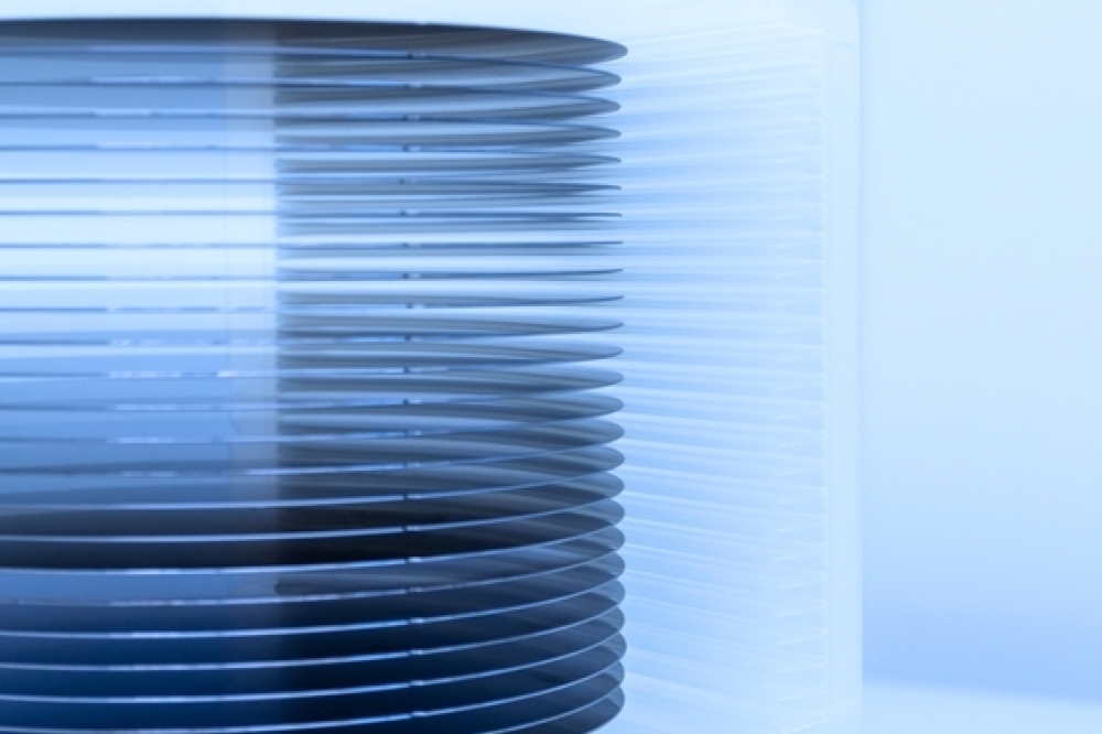
Figure 4. (Left) The ALD process shown diagrammatically. Precursors
adsorb and react in a layer-by-layer manner to build up films in steps
of individual atomic layers; (right) example of a fully automated ALD
tool, e.g., Oxford Instrument Plasma Technology’s ASP Cobra tool.
Over the past decade, a number of processing solutions have been developed to circumvent the inherent disadvantages arising from thermal oxidation. Efforts have focused on deposition-based processes, such as atomic layer deposition (ALD) and low-pressure CVD. With these approaches, the entire oxidation process is based entirely on the chemical reaction between silicon and oxygen precursors, with no consumption of the underlying SiC or residual carbon at the interface.
Our team, a partnership between Warwick University, Warwick Manufacturing Group and Oxford Instruments, is developing one such process. Our solution for improved gate oxide reliability focuses on ALD.
Controlling conformal depositions
All ALD processes involve the delivery of one precursor into the chamber in a short pulse. This precursor is adsorbed onto the samples surface, with molecules remaining on the surface after the pulse is complete. A second precursor is then pulsed into the chamber. This additional precursor reacts with the adsorbed layer, ideally to form a single atomic layer of the desired material. Unlike thermal oxidation, this approach avoids any consumption of the underlying semiconductor material. Cycling of this process stops after reaching the desired oxide thickness.
Unfortunately, as is the case with as-grown thermal layers, the quality of the as-deposited gate dielectrics is not ideal. Weaknesses include high leakage currents, large hysteresis voltages and substantial mobile charges in the oxides. To address these issues, it’s the norm to anneal the dielectric in a furnace heated to between 1000 °C and 1200 °C. While an inert gas such as argon is commonly used for the post-process anneal, forming gas adds 5 percent hydrogen for reducing chemistry, in contrast to the oxidising chemistry of NO and N2O (see Figure 4 for an illustration of the current state of the art).

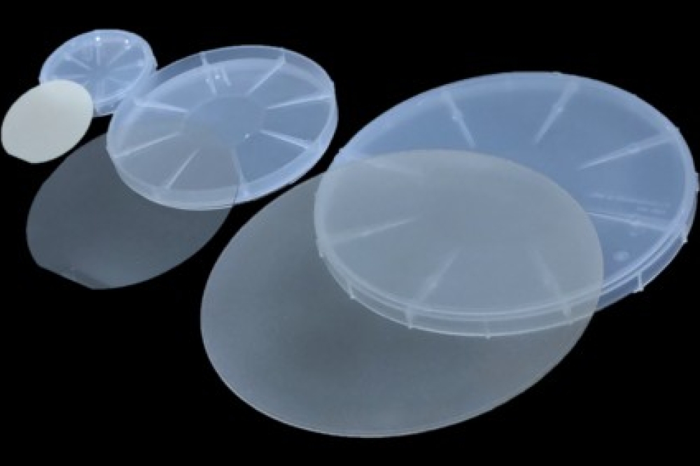
Figure 5. (Left) RCA clean of an 200 mm SiC wafer prior to device
fabrication and (Right) Optical microscopy inspection of a fully
patterned 150 mm SiC MOSFET wafer, showing multiple test cells.
Our team has spent several years developing SiC MOSFETs with low channel resistances. This can be achieved with a fully automated ALD kit produced by Oxford Instruments.
We have taken a slightly different approach from the one that most commercial entities would have pursued, deciding to shy away from using thermal oxides. We have avoided them because our view is that a deposition-based process is better suited to realising high channel mobilities – it offers greater control, as well as the opportunity to draw on the wealth of experience from very similar silicon passivation techniques that have been used to improve the interface.
Our approach begins with the deposition of a 40-50 nm-thick SiO2 layer by ALD, followed by annealing for 1 hour in forming gas at 1,100 °C. More details of our process have been reported in the papers listed in the reading list at the end of this article (see (Figure 5 (a)) for a picture of a 200 mm wafer during the RCA 1 & 2 standard clean, and a fully patterned wafer during inspection (see Figure 5 (b)).
Measurements of the electrical characteristics of our devices have produced excellent results. In our lateral MOSFETs, the maximum field-effect mobility is 110 cm2 V-1 s-1 (see Figure 7 (a), outperforming any commercially available SiC MOSFET. If industrial producers of SiC MOSFETs adopt our process, they could trim the total specific on-resistance by more than 10 percent, and have the opportunity for a die shrink while maintaining the blocking voltage and current rating.
When introducing any new processing technology, there is a need to assess whether it has any impact on device reliability. To investigate this, we began by stressing our power devices at constant voltages until we detect oxide breakdown (see Figure 6 for the test setup for static characterisation of our SiC devices).

Figure 6. Quarter of a 150 mm MOSFET wafer on a Semiprobe
semi-automatic probe station. Measurements were carried out using a
Keysight B1505A parameter analyser. Automated measurements connecting
both the stage and analyser were programmed using standard LabView
software.
Compared with the more conventional approaches to forming an oxide, such as direct thermal growth or low-pressure CVD, gate oxides produced with our ALD process consistently show the most promising results. Our extracted channel mobilities offer a path to lower-resistance MOSFETs (see Figure 7 (a)), and we realise the best breakdown performance, allowing devices to be stressed at higher voltages before they fail (see Figure 7(b), which shows the current-voltage results of the investigated devices). What’s more, our MOSFETs are more robust, evidenced by the longer time that a device can be stressed before it breaks down (see Figure 7 (c)). Extrapolations from stress tests at multiple electric fields demonstrate that our devices can operate at higher voltages while providing the same lifetime as their thermally oxidised counterparts.
To put our efforts into perspective, let’s consider the planar 1.2 kV SiC MOSFET. When produced with our process, this device can operate at higher electric fields, provide a reduction in on-resistance by 30 percent, and guarantee a sufficient dielectric lifetime.

Figure 7. (Top) Extracted channel mobility of a representative lateral
MOSFET structure with a channel length of 100 µm. (Middle) I-V
measurements of the investigated samples at 175 °C with a device area of
3.14 x 10⁻⁴ cm2. (Bottom) Time to breakdown
versus applied voltage/electric field of measured devices. It is evident
that the presented deposited oxides offer a path towards more reliable
SiC products.
How does it work?
An immense advantage of our collaboration is that we have access to world-leading physical characterisation expertise, as well as a direct pathway to the market.
Over the last ten years there has been the development of the Warwick Photoemission Research Technology Platform under the leadership of Marc Walker, a co-author of this feature. This suite of photoemission kit, which can be applied to semiconductor interface analysis, includes X-ray photoelectron spectroscopy specifically tailored towards the analysis of the SiC MOSFET, including the SiO2/SiC interfaces.
One of the strengths of X-ray photoelectron spectroscopy is that it can be used to analyse the chemical bonding environment at the SiO2/SiC interface. By comparing thermally oxidised and ALD-deposited oxides with this form of spectroscopy, we can reveal potential approaches to passivate defects.
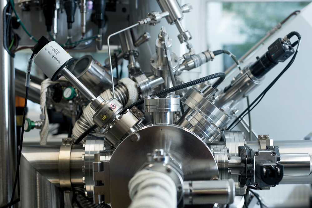
With our Kratos Axis Ultra delay-line detector and ScientaOmicron multiprobe instruments, we are gaining additional insight into the origins of improvement brought about by the ALD process (see Figure 8 (a)). With this tool we have been able to determine whether an interface is richer in silicon or carbon by looking at the stoichiometric ratio of Si-C in the silicon 2p spectrum and C-Si in the carbon 1s spectrum.
This approach has revealed a C:Si ratio below 1 for all deposited samples, indicating that the interface is silicon-rich. Our samples produced using ALD and a forming gas anneal have the most silicon-rich bonding environment (see Figure 8 (b)). Previous work from our group has established that this arises from the creation of a silicon-rich environment near the interface after ALD deposition of SiO2, a situation that makes it easier to passivate silicon dangling bonds.

Figure 8. (Left) The Scienta r4000 ARPES analyser mounted on the ScientaOmicron multiprobe photoemission system. Samples are illuminated with Al Ka X-rays. Any spectra were analysed at take-off angles of 90 ° and 15 °, giving a measurement depth of 10 nm and 3 nm, respectively. Photoelectrons were detected in the SPHERA hemispherical analyser mounted on the same instrument, and on the Kratos Axis Ultra DLD instrument (not shown). (Right) Extracted C:Si ratios of the investigated samples.
Alongside the revealing X-ray photoelectron spectroscopy analysis, our team has employed transmission electron microscopy to scrutinise the sharpness, cleanliness, chemical composition and, generally, the quality of the oxide/semiconductor interface (see Figure 9 (a) for an image of our scanning transmission electron microscope, the Thermo Scientific Talos F200X).
Using our scanning transmission electron microscope, we have undertaken structural and chemical analysis of our samples with sub-nanometre resolution. Operating at 200 kV, the F200X delivers high-resolution imaging in both transmission electron microscopy and scanning transmission electron microscope modes with a spatial resolution smaller than 0.14 nm. This instrument also provides fast, precise chemical mapping, using the Super-X quad energy dispersive X-ray spectroscopy detectors.
After preparing our samples with a focused-ion beam scanning electron microscope (see Figure 9 (b), we loaded them into the F200X to investigate the interfaces. We were keen to determine the presence of materials, the order of the semiconductor-oxide transition, and to see if there were any obvious surface decorations. We are encouraged by our findings, which reveal that our annealed gate dielectric formed by ALD has excellent interface quality.

Figure 9. (Left) Thermo Scientific Talos F200X scanning transmission
electron microscope. (Right) Sample after thinning back by means of
focused-ion beam scanning electron microscope.
Our research has demonstrated the value and readiness of ALD gate dielectrics on SiC. Channel mobility and reliability analysis shows substantial improvements on the current state of the art. Physical characterisation has identified a chemical foundation of the performance gains and excellent physical morphology. The superb controllability of ALD processes offers further scope to improve gate oxide, on-resistance, yield and cost. Our next step is to perform a pilot of the process and verify its reliability in commercial devices, paving the way to large-scale production.
•The authors wish to thank Marc Walker, Akif Yildirim, Gerard Colston, Qinze Cao, Kyrylo Melnyk, Xinkai Tian and Richard Jefferies from the University of Warwick, Geoff West from Warwick Manufacturing Group and Grant Baldwin from Oxford Instruments Plasma Technology.