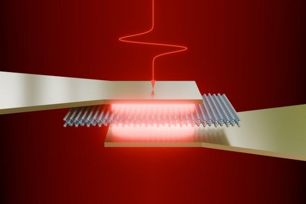
Three-terminal GaN diode boosts optoelectronic performance
Opens new possibilities for using external electric fields to control carrier transport during light emission or detection processes
Photodiodes are fundamental components in everything from LEDs to detectors. However, the traditional approach of employing external driving circuits alongside photodiodes can hamper signal transmission speed, bandwidth, and system integration.
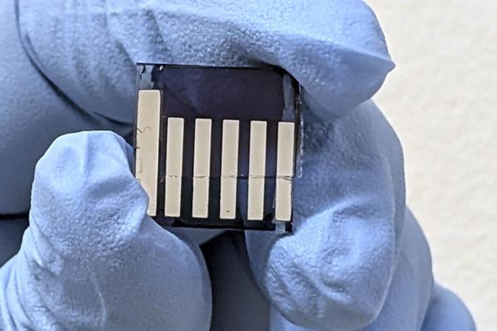
In response to these challenges, Sun Haiding’s iGaN Lab at the University of Science and Technology of China (USTC) in collaboration with Liu Sheng’s team from Wuhan University have integrated a third terminal directly onto a GaN-based p-n diode. Their research paper 'A three-terminal light emitting and detecting diode' was published in April 2024 in Nature Electronics.
The approach enables the modulation of carrier behaviour through an external electric field, thereby offering effective control over the optoelectronic characteristics of the diode. The integration of traditional photodiodes with a metal-oxide-semiconductor (MOS) structure in a compact on-chip device opens new possibilities for using external electric fields to control carrier transport during light emission or detection processes.
Beyond facilitating tunable light emission and multifunctional optoelectronic detection, this innovation could enhance the performance and versatility of optical communication systems, according to the researchers. By reducing reliance on external driving circuits, the three-terminal diode enables higher bandwidth and miniaturisation, thus paving the way for more efficient and compact optical communication solutions.
Moreover, its application extends to reconfigurable optoelectronic logic gates, empowering the development of high-speed integrated chips capable of adapting to diverse operational requirements without the need for structural modifications.
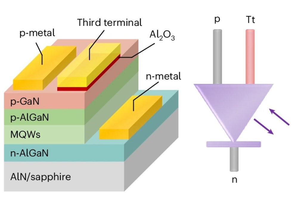
Pictured above: Schematic structure of the three terrminal diode and a symbol representing the emitter and detector.