Tiny device could lead better lasers

Researchers use perovskite to create first topological quantum simulator
Researchers at Rensselaer Polytechnic Institute in the US have made a tiny device that will help physicists investigate the fundamental nature of matter and light. Their findings, published in the journal Nature Nanotechnology, could also support the development of more efficient lasers used in fields ranging from medicine to manufacturing.
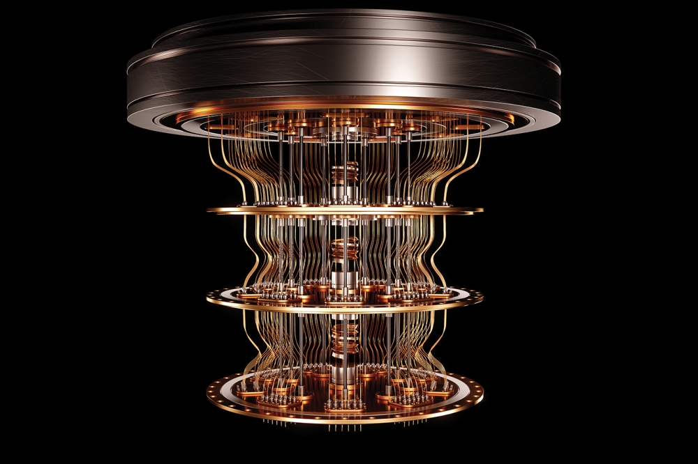
The device is made of a photonic topological insulator. A photonic topological insulator can guide photons to interfaces specifically designed within the material while also preventing these particles from scattering through the material itself.
Because of this property, topological insulators can make many photons coherently act like one photon. The devices can also be used as topological 'quantum simulators' miniature laboratories where researchers can study quantum phenomenon, the physical laws that govern matter at very small scales.
“The photonic topological insulator we created is unique. It works at room temperature. This is a major advance. Previously, one could only investigate this regime using big, expensive equipment that super cools matter in a vacuum. Many research labs do not have access to this kind of equipment, so our device could allow more people to pursue this kind of basic physics research in the lab,” said Wei Bao, assistant professor in the Department of Materials Science and Engineering at RPI and senior author of the Nature Nanotechnology study.
“It is also a promising step forward in the development of lasers that require less energy to operate, as our room-temperature device threshold — the amount of energy needed to make it work — is seven times lower than previously developed low-temperature devices,” Bao added.
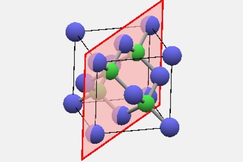
To create their device, the researchers grew ultrathin plates of halide perovskite, a crystal made of cesium, lead, and chlorine, and etched a polymer on top of it with a pattern. They sandwiched these crystal plates and polymer between sheets of various oxide materials, eventually forming an object about 2 microns thick and 100 microns in length and width.
When the researchers shined a laser light on the device, a glowing triangular pattern appeared at the interfaces designed in the material. This pattern, dictated by the device’s design, is the result of topological characteristic of lasers.
“Being able to study quantum phenomena at room temperature is an exciting prospect. Professor Bao’s innovative work shows how materials engineering can help us answer some of science’s biggest questions,” said Shekhar Garde, dean of the RPI School of Engineering.
The study was primarily supported by grants from the National Science Foundation and Office of Naval Research.